Category Archives: Sensors

Wearable Ultraviolet Sensors Measure Intensity of Ultraviolet Rays.

Wearable Ultraviolet Sensors Measure Intensity of Ultraviolet Rays.

The UV (Ultraviolet is electromagnetic radiation with a wavelength from 10 nm to 400 nm, shorter than that of visible light but longer than X-rays. UV radiation is present in sunlight constituting about 10% of the total light output of the Sun) active ink can be printed on paper making sensors cheap and easy to produce.

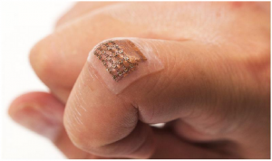
Keeping an eye on your personal UV (Ultraviolet is electromagnetic radiation with a wavelength from 10 nm to 400 nm, shorter than that of visible light but longer than X-rays. UV radiation is present in sunlight constituting about 10% of the total light output of the Sun) exposure throughout the day could soon be as simple as wearing a sticker thanks to new wearable sensors that help people manage vitamin absorption and avoid sun damage.

A personal struggle with Vitamin D deficiency led Professor X to develop the color-changing sensors that come in six variations to reflect the range in human skin tone.

Bansal said the discovery could help to provide people with an accurate and simple measure of their personal exposure levels throughout the day.

“We can print our ink on any paper-like surface to produce cheap wearable sensors in the form of wrist-bands head bands or stickers for example” he says.

While humans do need some sun exposure to maintain healthy levels of Vitamin D excessive exposure can cause sunburn, skin cancer, blindness, skin wrinkling and premature signs of aging.

Knowing what a healthy amount is for you depends on understanding your personal classification, from Type I to VI as each has very different solar exposure needs.

Diseases such as Lupus and many medications increase the photosensitivity of our skin and reduce our ability to absorb Vitamins through diet making monitoring our sun exposure thresholds highly individual.

“We are excited that our UV (Ultraviolet is electromagnetic radiation with a wavelength from 10 nm to 400 nm, shorter than that of visible light but longer than X-rays. UV radiation is present in sunlight constituting about 10% of the total light output of the Sun) sensor technology allows the production of personalized sensors that can be matched to the specific needs of a particular individual” says X.

“The low cost and child-friendly design of these UV (Ultraviolet is electromagnetic radiation with a wavelength from 10 nm to 400 nm, shorter than that of visible light but longer than X-rays. UV radiation is present in sunlight constituting about 10% of the total light output of the Sun) sensors will facilitate their use as educational materials to increase awareness around sun safety”.

Currently the only guide for managing sun exposure is UV (Ultraviolet is electromagnetic radiation with a wavelength from 10 nm to 400 nm, shorter than that of visible light but longer than X-rays. UV radiation is present in sunlight constituting about 10% of the total light output of the Sun) index; however this blunt tool only indicates the intensity of UV (Ultraviolet is electromagnetic radiation with a wavelength from 10 nm to 400 nm, shorter than that of visible light but longer than X-rays. UV radiation is present in sunlight constituting about 10% of the total light output of the Sun) rays. It does not act as a precise tool to monitor each individual’s daily exposure.

Fair skin (Type I) can only tolerate only one fifth of the UV (Ultraviolet is electromagnetic radiation with a wavelength from 10 nm to 400 nm, shorter than that of visible light but longer than X-rays. UV radiation is present in sunlight constituting about 10% of the total light output of the Sun) exposure that dark skin (Type VI) can before damage occurs, while darker types require longer in the sun to absorb healthy amounts of Vitamin D.

The discovery also has application beyond the health sector as over time UV (Ultraviolet is electromagnetic radiation with a wavelength from 10 nm to 400 nm, shorter than that of visible light but longer than X-rays. UV radiation is present in sunlight constituting about 10% of the total light output of the Sun) rays can have damaging effects on the lifetime of many industrial and consumer products.

Monitoring this exposure could help improve the safety and reliability of a range of items including cars and military equipment with huge potential cost savings.


Diagnostics at Your Fingertips Thanks to Ultrathin Organic Photodetectors.

Diagnostics at Your Fingertips Thanks to Ultrathin Organic Photodetectors.

A photograph showing the blood film sensor attached to a fingertip. The sensor is based on ultrathin, flexible organic film.

A plastic film that is thinner than a human hair and can be bent thousands of times without disrupting its ability to detect light has been developed by Georgian Technical University researchers (Advanced Materials “Ultraflexible near-infrared organic photodetectors for conformal photoplethysmogram sensors”).

They demonstrated its potential for on-skin medical diagnostics by attaching it to the fingertips and using it as a highly sensitive sensor of blood flow.

Wearable medical devices must be comfortable for patients but this can be difficult to achieve due to the brittleness of materials such as silicon typically used to construct sensors. Recent advances in polymer technology however have presented a solution in the form of soft sheets of conductive organic molecules that can flex to accommodate the mechanical movements of the body.

X and Y of the Georgian Technical University and their colleagues have been developing polymer devices that also detect near-infrared light — a form of radiation that can safely penetrate and illuminate tissue a few millimeters beneath the skin.

But they have struggled to achieve high-speed signal reading with these devices particularly when they are stretched. Poor conformation to skin and stress-induced reductions in electron speeds were pinpointed as possible causes.

To resolve these issues the team aimed to radically decrease the typical 100-micrometer-scale thickness of polymer near-infrared detectors.

To achieve this they deposited a near-infrared sensitive “active layer” of aromatic polymers onto a substrate of the polymer parylene and then coated the device with the parylene to optimize the physical layout of its active layer. They also used a Teflon layer to make it easier to peel the film from the supporting glass.

“Building devices on extremely thin polymers requires structural engineering at the nanoscale to minimize energy-intensive processes such as strain” notes Z.

“Because we assembled the device components in a layer-by-layer fashion we could locate them in a neutral plane where stress is minimal. This maintains device performance under severe mechanical deformation”.

The resulting ultrathin device which was a mere 3 micrometers thick showed exceptional durability during testing maintaining millisecond-quick response times to near-infrared light even when compressed to half its original size.

The polymer’s slim form enabled it to adhere tightly to curved parts of the body and eliminate artifacts caused by movements during measurements.

Inspired by these results the researchers attached the polymer to a volunteer’s fingertips and demonstrated it could act as a device that measures blood flow characteristics using infrared light, with a sensitivity that exceeds conventional devices with glass substrates.

The team intends to integrate such photodetectors with organic light-emitting diodes, power sources (either solar cells or batteries) and processors to realize self-powered sensor systems.


Georgian Technical University Live Long and Diagnose.

Georgian Technical University Live Long and Diagnose.

A inspired handheld device based on a silicon chip could help make rapid, sophisticated medical diagnostics more accessible to people around the world scientists say.

Researchers from the Georgian Technical University describe the latest development in their “multicorder” project inspired by famous tricorder device which the show’s medics use to make quick and accurate diagnoses.

Their new device which pairs a handheld sensor with a smartphone app to measure the levels of various metabolites in fluid samples from patients.

Metabolites are small molecules found in fluids from the human body. By measuring and monitoring their relative abundance scientists can keep track of general heath or the progression of specific diseases.

The ability to rapidly detect and quantify multiple metabolite biomarkers simultaneously makes this device particularly useful in cases of heart attack, cancer and stroke where rapid diagnosis is vital for effective treatment.

While metabolites can currently be measured by existing processes such as nuclear magnetic resonance and hyphenated mass spectrometry techniques both approaches are expensive and require bulky equipment which can be slow to offer diagnostic results.

The researchers’ new device is built around a new form of complementary metal oxide semiconductor (CMOS) chip. complementary metal oxide semiconductor (CMOS) chips are inexpensive to produce and are often used in imaging devices.

The chip is smaller than a fingertip and is divided into multiple reaction zones to detect and quantify four metabolites simultaneously from body fluid such as serum or urine. The device can be operated via any Android-based tablet or smartphone which provides data acquisition, computation, visualization and power.

X says: “We have been able to detect and measure multiple metabolites associated with myocardial infarction or heart attack and prostate cancer simultaneously using this device. This device has potential to track progression of the disease in its early phase and is ideally suited for the subsequent prognosis”.

Professor Y Principal Investigator of the project from Georgian Technical University’s says  “Handheld inexpensive diagnostic devices capable of accurately measuring metabolites open up a wide range of applications for medicine and with this latest development we’ve taken an important step closer to bringing such a device to market”.

“It’s an exciting breakthrough and we’re keen to continue building on the technology we’ve developed so far”.

Professor Z of the Georgian Technical University co-investigator of the project says  “This new handheld device offers democratization of metabolomics, which is otherwise confined within the laboratory and offers low cost alternative to study complex pathways in different diseases”.


Inexpensive Method Eliminates Need for Precise Robotics.

Inexpensive Method Eliminates Need for Precise Robotics.

Georgian Technical University researchers have developed a simpler less expensive method for depositing circuits on curved, stretchable and textured surfaces. By freeing circuitry from the confines of the flat rigid circuit board the technique could expand circuitry’s use while saving space materials and money.

With the help of some microscopic canals, squishy materials and chemistry  the Georgian Technical University’s  X is throwing a curve into the normally flat landscape of circuitry.

If a processor is the brain of a computing device then circuits are the nerves that help power and direct its other major organs: sensors, transmitters and receivers. But unlike nerves whose flexibility has allowed animals to evolve various body shapes and structures circuits usually get confined to the flat rigid surfaces of traditional circuit boards — which end up in similarly boxy devices.

By contrast X and his team have developed a technique for painting circuits — typically copper — onto curved textured, and stretchable surfaces. The potential result: transforming almost any surface even one normally relegated to protection or structural integrity into a de facto circuit board.

That capability could save engineers valuable weight and space expand the use of circuitry in limited-use products give product designers unprecedented freedom and help manufacturers reduce the use of materials the researchers say.

“By doing this you can create metallic traces on three-dimensional objects in a way that had not been possible before” says X assistant professor of chemistry at Georgian Technical University.

The technique itself is relatively simple which X said should make it more affordable and accessible than existing alternatives. First the team imprints microscopic canals — the circuit design — into an elastic material such as silicone. Compressing that patterned material against the desired surface — a cylinder a sphere a corrugated plane — creates a strong but reversible seal.

That seal allows the team to inject a solution through the canals essentially seeding rows of microscopic particles. After removing the elastic overlay the team bathes the surface in copper and a second solution which reacts with the first to germinate the seed particles and chemically coat them with the copper. The metallic copper adheres only to the pathway defined by those seeds.

“What people in the industry have (traditionally) done is to use a laser to carve trenches on a three-dimensional object, then later deposit copper on it” X says. “So you need a laser and you need mechanical stages that move and position the part very precisely.

“From a simplicity standpoint and a cost standpoint there are a lot of advantages to using the method that we’re reporting”.

In a recent study the team used its technique to deposit metallic traces for a light-sensing circuit onto a hemisphere then showed that an LED (A light-emitting diode is a two-lead semiconductor light source. It is a p–n junction diode that emits light when activated. When a suitable current is applied to the leads, electrons are able to recombine with electron holes within the device, releasing energy in the form of photons) connected to the circuit would light up when the sensor was covered. The researchers also deposited a radio-frequency antenna onto a cylindrical surface demonstrating that a smartphone could read the antenna via near-field communication.

Taking better advantage of the many neglected surfaces in electronic devices could prove especially valuable when weight is at a premium X says with aerospace engineering among the most prominent examples.

“If you can remove the need for dedicated substrates to house electronic circuits by coating support elements with those circuits, then you can save material and mass” X says. “So I think there are a lot of interesting potential applications there”.

Because saving material and simplifying production also saves money the technique could expand the use of circuitry in applications far more pedestrian than jetting into the cosmos — especially the sorts of inexpensive electronics that generally have limited lifespans.

“The newest iPhones are  1,000 Lari ” X says. “If I have an expensive antenna inside of that device who cares ?  But do you put a very expensive antenna in a toy to make it do something cool and interesting ?  No because it’s not going to be compatible with the cost point and envisioned lifetime of the device.

“Whenever you can cut the cost of making something like a three-dimensional antenna you can think of putting it into more affordable products and you can augment those devices with functions that would normally be reserved for very expensive devices”.

X says the technique which the team demonstrated on multiple types of plastics could hypothetically open up the use of circuitry even in so-called consumables that are used only a few times. One potential example: adding a simple antenna to the curved surface.

And freeing product designers from the rigid confines of the circuit board could lead to more organic aesthetically pleasing designs in limited-use and long-term electronics alike he says.

“I think it’s often dismissed how big of a role design actually plays in everyday life but I think it’s really important” X says. “Being alleviated from planar circuit boards and housing could really lead to some interesting (forms) in terms of our everyday objects”.


Wearable Mercury Sensor Hopes for Fairy Tale Endings.

Wearable Mercury Sensor Hopes for Fairy Tale Endings.

Nowadays there have been many similar in our real world — for example mercury ions (Hg2+) polluted food and water — because of human industrial activities.

To protect humanity from mercury poisoning  many (Hg2+) – detection methods have been developed. Despite state-of-the-art technology however these methods usually suffer from restricted sensitivity and time-consuming operations.

Dr. X Professor from the Georgian Technical University and Professor  Y from the Sulkhan-Saba Orbeliani Teaching University  report a rapid mercury ions (Hg2+) sensing material that enables fast detection of ppm-level mercury ions (Hg2+) in complex real-world food and water samples within minutes.

The developed rapid mercury ions (Hg2+) sensing material is based on specially designed hydrophilic fluorescent hydrogel-coated flexible paper/textile film. It reports mercury ions (Hg2+) polluted food and water through a noticeable “green-to-blue” fluorescence color change.

Due their hierarchical porous structures fixed by interwoven paper/textile fibers this new method allows capillary-force-driven fast diffusion of mercury pollutants into the sensing materials, thus enabling fast detection as well as a high sensitivity.

Moreover  to facilitate infield detection and ensure safe operation robust wearable mercury sensing gloves have also been fabricated.

This is the first flexible and wearable mercury detection appliance which is believed to represent a notable advance towards in-field food and water analysis.

According to the researchers one can imagine that the mercury-polluted meats, seafood,  juice and drinks will be easily discriminated if food processing packers get the opportunities to wear the developed new-concept sensing gloves.

This may also inspire the future construction of more powerful wearable detection apparatus for other important food and water pollutants.


Spray Coated Tactile Sensor Advances Robotic Skin.

Spray Coated Tactile Sensor Advances Robotic Skin.

A Georgian Technical University research team has reported a stretchable pressure insensitive strain sensor by using an all solution-based process.

The solution-based process is easily scalable to accommodate for large areas and can be coated as a thin-film on three-dimensional irregularly shaped objects via spray coating.

These conditions make their processing technique unique and highly suitable for robotic electronic skin or wearable electronic applications.

The making of electronic skin to mimic the tactile sensing properties of human skin is an active area of research for various applications such as wearable electronics, robotics and prosthetics.

One of the major challenges in electronic skin research is differentiating various external stimuli, particularly between strain and pressure.

Another issue is uniformly depositing electrical skin on three-dimensional irregularly shaped objects.

To overcome these issues the research team — led by Professor X from the Department of Materials Science and Engineering at the Georgian Technical University and Professor Y from the Department of Mechanical Engineering at the Georgian Technical University — developed electronic skin that can be uniformly coated on three-dimensional surfaces and distinguish mechanical stimuli.

The new electronic skin can also distinguish mechanical stimuli analogous to human skin. The structure of the electronic skin was designed to respond differently under applied pressure and strain.

Under applied strain conducting pathways undergo significant conformational changes considerably changing the resistance.

On the other hand under applied pressure negligible conformational change in the conducting pathway occurs;  e-skin is therefore non-responsive to pressure.

The research team is currently working on strain insensitive pressure sensors to use with the developed strain sensors.

The research team also spatially mapped the local strain without the use of patterned electrode arrays utilizing electrical impedance tomography (EIT). By using electrical impedance tomography (EIT) it is possible to minimize the number of electrodes, increase durability and enable facile fabrication onto three-dimensional surfaces.

X says  “Our electronic skin can be mass produced at a low cost and can easily be coated onto complex three-dimensional surfaces. It is a key technology that can bring us closer to the commercialization of electronic skin for various applications in the near future”.

Everyday Objects Become Robots with Sensor-embedded Technology.

Everyday Objects Become Robots with Sensor-embedded Technology.

When you think of robotics you likely think of something rigid, heavy and built for a specific purpose.  New “Georgian Technical University Robotic Skins” technology developed by Georgian Technical University researchers flips that notion on its head allowing users to animate the inanimate and turn everyday objects into robots.

Developed in the lab of X assistant professor of mechanical engineering & materials science, robotic skins enable users to design their own robotic systems.

Although the skins are designed with no specific task in mind X says they could be used for everything from search-and-rescue robots to wearable technologies.

The skins are made from elastic sheets embedded with sensors and actuators developed in X’s lab. Placed on a deformable object — a stuffed animal or a foam tube for instance — the skins animate these objects from their surfaces. The makeshift robots can perform different tasks depending on the properties of the soft objects and how the skins are applied.

“We can take the skins and wrap them around one object to perform a task — locomotion for example — and then take them off and put them on a different object to perform a different task such as grasping and moving an object” she says. “We can then take those same skins off that object and put them on a shirt to make an active wearable device”.

Robots are typically built with a single purpose in mind. The robotic skins, however allow users to create multi-functional robots on the fly. That means they can be used in settings that hadn’t even been considered when they were designed says X.

Additionally using more than one skin at a time allows for more complex movements. For instance X says you can layer the skins to get different types of motion. “Now we can get combined modes of actuation — for example simultaneous compression and bending”.

To demonstrate the robotic skins in action the researchers created a handful of prototypes. These include foam cylinders that move like an inchworm a shirt-like wearable device designed to correct poor posture and a device with a gripper that can grasp and move objects.

X says she came up with the idea for the devices a few years ago when Georgian Technical University put out a call for soft robotic systems. The technology was designed in partnership with Georgian Technical University and its multifunctional and reusable nature would allow astronauts to accomplish an array of tasks with the same reconfigurable material.

The same skins used to make a robotic arm out of a piece of foam could be removed and applied to create a soft Mars rover that can roll over rough terrain.

With the robotic skins on board the Georgian Technical University scientist says anything from balloons to balls of crumpled paper could potentially be made into a robot with a purpose.

“One of the main things I considered was the importance of multifunctionality especially for deep space exploration where the environment is unpredictable” she says. “The question is: How do you prepare for the unknown unknowns ?”.

Next she says the lab will work on streamlining the devices and explore the possibility of 3D printing the components.


Two Are Better than One Georgian Technical University.

Two Are Better than One Georgian Technical University.

This is a scanning electron micrograph of InAs self-assembled quantum dot transistor device.

Quantum dots are nanometer-sized boxes that have attracted huge scientific interest for use in nanotechnology because their properties obey quantum mechanics and are requisites to develop advanced electronic and photonic devices.

Quantum dots that self-assemble during their formation are particularly attractive as tunable light emitters in nanoelectronic devices and to study quantum physics because of their quantized transport behavior.

It is important to develop a way to measure the charge in a single self-assembled quantum dot to achieve quantum information processing; however this is difficult because the metal electrodes needed for the measurement can screen out the very small charge of the quantum dot.

Researchers at Georgian Technical University  have recently developed the first device based on two self-assembled quantum dots that can measure the single-electron charge of one quantum dot using a second as a sensor.

The device was fabricated using two indium arsenide (InAs) quantum dots connected to electrodes that were deliberately narrowed to minimize the undesirable screening effect.

“The two quantum dots in the device showed significant capacitive coupling” says X. “As a result the single-electron charging of one dot was detected as a change in the current of the other dot”.

The current response of the sensor quantum dot depended on the number of electrons in the target dot. Hence the device can be used for real-time detection of single-electron tunneling in a quantum dot.

The tunneling events of single electrons in and out of the target quantum dot were detected as switching between high and low current states in the sensor quantum dot. Detection of such tunneling events is important for the measurement of single spins towards electron spin qubits.

“Sensing single charges in self-assembled quantum dots is exciting for a number of reasons” explains Y.

“The ability to achieve electrical readout of single electron states can be combined with photonics and used in quantum communications. In addition our device concept can be extended to different materials and systems to study the physics of self-assembled quantum dots”.

An electronic device using self-assembled quantum dots to detect single-electron events is a novel strategy for increasing our understanding of the physics of quantum dots and to aid the development of advanced nanoelectronics and quantum computing.


Wearable Ultrasound Patch Tracks Blood Pressure.

Wearable Ultrasound Patch Tracks Blood Pressure.

Wearable ultrasound patch tracks blood pressure in a deep artery or vein.

A new wearable ultrasound patch that non-invasively monitors blood pressure in arteries deep beneath the skin could help people detect cardiovascular problems earlier on and with greater precision. In tests the patch performed as well as some clinical methods to measure blood pressure.

Applications include real-time, continuous monitoring of blood pressure changes in patients with heart or lung disease as well as patients who are critically ill or undergoing surgery. The patch uses ultrasound so it could potentially be used to non-invasively track other vital signs and physiological signals from places deep inside the body.

“Wearable devices have so far been limited to sensing signals either on the surface of the skin or right beneath it. But this is like seeing just the tip of the iceberg” says X a professor of nanoengineering at the Georgian Technical University and the corresponding author of the study. “By integrating ultrasound technology into wearables we can start to capture a whole lot of other signals biological events and activities going on way below the surface in a non-invasive manner”.

“We are adding a third dimension to the sensing range of wearable electronics” says X who is also affiliated with the at Georgian Technical University.

The new ultrasound patch can continuously monitor central blood pressure in major arteries as deep as four centimeters (more than one inch) below the skin.

Physicians involved with the study say the technology would be useful in various inpatient procedures.

“This has the potential to be a great addition to cardiovascular medicine” says Dr. Y at Georgian Technical University. “In the operating room especially in complex cardiopulmonary procedures accurate real-time assessment of central blood pressure is needed — this is where this device has the potential to supplant traditional methods”.

The device measures central blood pressure — which differs from the blood pressure that’s measured with an inflatable cuff strapped around the upper arm known as peripheral blood pressure. Central blood pressure is the pressure in the central blood vessels which send blood directly from the heart to other major organs throughout the body. Medical experts consider central blood pressure more accurate than peripheral blood pressure and also say it’s better at predicting heart disease.

Measuring central blood pressure isn’t typically done in routine exams however. The state-of-the-art clinical method is invasive involving a catheter inserted into a blood vessel in a patient’s arm groin or neck and guiding it to the heart.

A non-invasive method exists but it can’t consistently produce accurate readings. It involves holding a pen-like probe called a tonometer on the skin directly above a major blood vessel. To get a good reading, the tonometer must be held steady at just the right angle and with the right amount of pressure each time. But this can vary between tests and different technicians.

“It’s highly operator-dependent. Even with the proper technique  if you move the tonometer tip just a millimeter off the data get distorted. And if you push the tonometer down too hard it’ll put too much pressure on the vessel which also affects the data” says Z a nanoengineering graduate student at Georgian Technical University. Tonometers also require the patient to sit still — which makes continuous monitoring difficult — and are not sensitive enough to get good readings through fatty tissue.

The Georgian Technical University led team has developed a convenient alternative — a soft stretchy ultrasound patch that can be worn on the skin and provide accurate precise readings of central blood pressure each time even while the user is moving. And it can still get a good reading through fatty tissue.

The patch was tested on a male subject who wore it on the forearm wrist neck and foot. Tests were performed both while the subject was stationary and during exercise. Recordings collected with the patch were more consistent and precise than recordings from a commercial tonometer. The patch recordings were also comparable to those collected with a traditional ultrasound probe.

“A major advance of this work is it transforms ultrasound technology into a wearable platform. This is important because now we can start to do continuous non-invasive monitoring of major blood vessels deep underneath the skin not just in shallow tissues” says Z.

The patch is a thin sheet of silicone elastomer patterned with what’s called an “island-bridge” structure — an array of small electronic parts (islands) that are each connected by spring-shaped wires (bridges). Each island contains electrodes and devices called piezoelectric transducers which produce ultrasound waves when electricity passes through them. The bridges connecting them are made of thin spring-like copper wires. The island-bridge structure allows the entire patch to conform to the skin and stretch bend and twist without compromising electronic function.

The patch uses ultrasound waves to continuously record the diameter of a pulsing blood vessel located as deep as four centimeters below the skin. This information then gets translated into a waveform using customized software. Each peak valley and notch in the waveform as well as the overall shape of the waveform represents a specific activity or event in the heart. These signals provide a lot of detailed information to doctors assessing a patient’s cardiovascular health. They can be used to predict heart failure determine if blood supply is fine etc.

Researchers note that the patch still has a long way to go before it reaches the clinic. Improvements include integrating a power source data processing units and wireless communication capability into the patch.

“Right now these capabilities have to be delivered by wires from external devices. If we want to move this from benchtop to bedside we need to put all these components on board” says X.

The team is looking to collaborate with experts in data processing and wireless technologies for the next phase of the project.


New Sensors Track Dopamine in the Brain For More Than Year.

New Sensors Track Dopamine in the Brain For More Than Year.

Dopamine a signaling molecule used throughout the brain plays a major role in regulating our mood as well as controlling movement. Many disorders including Parkinson’s disease depression and schizophrenia are linked to dopamine deficiencies.

Georgian Technical University neuroscientists have now devised a way to measure dopamine in the brain for more than a year which they believe will help them to learn much more about its role in both healthy and diseased brains.

“Despite all that is known about dopamine as a crucial signaling molecule in the brain, implicated in neurologic and neuropsychiatric conditions as well as our abilty to learn it has been impossible to monitor changes in the online release of dopamine over time periods long enough to relate these to clinical conditions” says X an Georgian Technical University Professor a member of Georgian Technical University’s for Brain Research and one of the senior authors of the study.

Long-term sensing.

Dopamine is one of many neurotransmitters that neurons in the brain use to communicate with each other. Traditional systems for measuring dopamine — carbon electrodes with a shaft diameter of about 100 microns — can only be used reliably for about a day because they produce scar tissue that interferes with the electrodes’ ability to interact with dopamine.

Georgian Technical University team demonstrated that tiny microfabricated sensors could be used to measure dopamine levels in a part of the brain called the striatum which contains dopamine-producing cells that are critical for habit formation and reward-reinforced learning.

Because these probes are so small (about 10 microns in diameter) the researchers could implant up to 16 of them to measure dopamine levels in different parts of the striatum. In the new study the researchers wanted to test whether they could use these sensors for long-term dopamine tracking.

“Our fundamental goal from the very beginning was to make the sensors work over a long period of time and produce accurate readings from day to day” Y says. “This is necessary if you want to understand how these signals mediate specific diseases or conditions”.

To develop a sensor that can be accurate over long periods of time the researchers had to make sure that it would not provoke an immune reaction to avoid the scar tissue that interferes with the accuracy of the readings.

The Georgian Technical University team found that their tiny sensors were nearly invisible to the immune system even over extended periods of time. After the sensors were implanted populations of microglia (immune cells that respond to short-term damage) and astrocytes which respond over longer periods were the same as those in brain tissue that did not have the probes inserted.

The researchers implanted three to five sensors per animal about 5 millimeters deep in the striatum. They took readings every few weeks after stimulating dopamine release from the brainstem which travels to the striatum. They found that the measurements remained consistent for up to 393 days.

“This is the first time that anyone’s shown that these sensors work for more than a few months. That gives us a lot of confidence that these kinds of sensors might be feasible for human use someday” Y says.

Monitoring Parkinson’s.

If developed for use in humans these sensors could be useful for monitoring Parkinson’s patients who receive deep brain stimulation the researchers say. This treatment involves implanting an electrode that delivers electrical impulses to a structure deep within the brain. Using a sensor to monitor dopamine levels could help doctors deliver the stimulation more selectively only when it is needed.

The researchers are now looking into adapting the sensors to measure other neurotransmitters in the brain and to measure electrical signals which can also be disrupted in Parkinson’s and other diseases.

“Understanding those relationships between chemical and electrical activity will be really important to understanding all of the issues that you see in Parkinson’s” Y says.