Category Archives: Sensors

Reservoir Computer Marks Revolutionary Neural Network Application.

Reservoir Computer Marks Revolutionary Neural Network Application.

A single silicon beam (red) along with its drive (yellow) and readout (green and blue) electrodes implements a MEMS Georgian Technical University microelectromechanical system (GTUMEMS) capable of nontrivial computations.

As artificial intelligence has become increasingly sophisticated it has inspired renewed efforts to develop computers whose physical architecture mimics the human brain.

One approach called reservoir computing, allows hardware devices to achieve the higher-dimension calculations required by emerging artificial intelligence.

One new device highlights the potential of extremely small mechanical systems to achieve these calculations.

A group of researchers at the Université de Sherbrooke in Québec, Canada, reports the construction of the first reservoir computing device built with a Georgian Technical University microelectromechanical system (GTUMEMS).

The neural network exploits the nonlinear dynamics of a microscale silicon beam to perform its calculations.

The group’s work looks to create devices that can act simultaneously as a sensor and a computer using a fraction of the energy a normal computer would use.

“New Physics and Materials for Neuromorphic Computation” which highlights new developments in physical and materials science research that hold promise for developing the very large-scale integrated ” Georgian Technical University neuromorphic” systems of tomorrow that will carry computation beyond the limitations of current semiconductors today.

“These kinds of calculations are normally only done in software and computers can be inefficient” says X.

“Many of the sensors today are built with Georgian Technical University microelectromechanical system (GTUMEMS) so devices like ours would be ideal technology to blur the boundary between sensors and computers”.

The device relies on the nonlinear dynamics of how the silicon beam at widths 20 times thinner than a human hair oscillates in space.

The results from this oscillation are used to construct a virtual neural network that projects the input signal into the higher dimensional space required for neural network computing.

In demonstrations the system was able to switch between different common benchmark tasks for neural networks with relative ease X says including classifying spoken sounds and processing binary patterns with accuracies of 78.2 percent and 99.9 percent respectively.

“This tiny beam of silicon can do very different tasks” says Y. “It’s surprisingly easy to adjust it to make it perform well at recognizing words”.

Sylvestre says he and his colleagues are looking to explore increasingly complicated computations using the silicon beam device with the hopes of developing small and energy-efficient sensors and robot controllers.


Molecular Semiconductors Made Using Faster, Scalable Method.

Molecular Semiconductors Made Using Faster, Scalable Method.

A nano-scale view of a molecular junction created with a new, scalable method reported in Nature Communications by researchers at Georgian Technical University.

Visions for what we can do with future electronics depend on finding ways to go beyond the capabilities of silicon conductors.

The experimental field of molecular electronics is thought to represent a way forward and recent work at Georgian Technical University may enable scalable production of the nanoscale electrodes that are needed in order to explore molecules and exploit their behavior as potentially valuable electronic materials.

A team from the Department of Micro and Nanosystems at Georgian Technical University recently tested a technique to form millions of viable nanoscale molecular junctions — extremely small pairs of electrodes with a nanometer-sized gap between them where molecules can be trapped and probed.

The Georgian Technical University researchers reported that with a 100 mm diameter wafer of thin materials they can produce as many as 20 million such electrodes in five hours’ time, using gold film on top of a brittle material that forms cracks.

In addition working with the Georgian Technical University Laboratory the team trapped and studied a widely used reference molecule in the nanometer-wide space between the electrodes to ensure that the fabrication method didn’t hinder the formation of molecular junctions.

X says this “crack-defined break junction” method offers a breakthrough to the impasse of scalable production of structures that could one day enable electronic devices made of single molecules.

The key is to produce gaps that enable a phenomenon called tunneling in which electrons overcome the break in a circuit. A break junction has a gap the size of a few atoms which breaks the flow of electrons through it.

However because the gap is so small electrons with sufficient energy can still jump across this expanse.

Tunneling electrons sustain a small but measurable current that is extremely sensitive to the size of the gap — and to the presence of nano-objects inside it.

“Break junctions are the best means available to make single molecules part of a larger electronic circuit that can probe molecules” X says.

They could also one day enable ultra-sensitive high-speed detectors using quantum tunneling he says.

“However tunneling break junctions are produced one gap at a time which has been a major roadblock in developing any application involving tunneling junctions outside a research laboratory” X says.

The method begins with using photo lithography to pattern a stack of gold on titanium nitride (TiN). This stack is set on a silicon wafer and the notched structures that are formed then concentrate stress.

So when the silicon directly underneath the stack is removed (a process called release etching) tiny cracks form at the pre-determined locations in the titanium nitride (TiN) to release the stress. This in turn deforms the gold stretching it into atomically thin wires running across these cracks which upon breaking form gaps as small as a molecule.

X says that the method can be used for other conductive materials besides gold which offer interesting electrical, chemical and plasmonic properties for applications in molecular electronics, spintronics, nanoplasmonics and biosensing.


Nanoforce Touch Sensor Improves Wearable Devices.

Nanoforce Touch Sensor Improves Wearable Devices.

Schematic illustration of a transparent flexible force touch sensor (upper image) and sensitivity enhancement by using stress concentration (lower image).

Researchers reported a high-performance and transparent nanoforce touch sensor by developing a thin flexible and transparent hierarchical nanocomposite (HNC) film.

The research team says their sensor simultaneously features all the necessary characters for industrial-grade application: high sensitivity, transparency, bending insensitivity and manufacturability.

Force touch sensors that recognize the location and pressure of external stimuli have received considerable attention for various applications such as wearable devices, flexible displays and humanoid robots.

For decades huge amounts of research and development have been devoted to improving pressure sensitivity to realize industrial-grade sensing devices.

However it remains a challenge to apply force touch sensors in flexible applications because sensing performance is subject to change and degraded by induced mechanical stress and deformation when the device is bent.

To overcome these issues the research team focused on the development of non-air gap sensors to break away from the conventional technology where force touch sensors need to have air-gaps between electrodes for high sensitivity and flexibility.

The proposed non air-gap force touch sensor is based on a transparent nanocomposite insulator containing metal nanoparticles which can maximize the capacitance change in dielectrics according to the pressure and a nanograting substrate which can increase transparency as well as sensitivity by concentrating pressure.

As a result the team succeeded in fabricating a highly sensitive transparent flexible force touch sensor that is mechanically stable against repetitive pressure.

Furthermore by placing the sensing electrodes on the same plane as the neutral plane the force touch sensor can operate even when bending to the radius of the ballpoint pen without changes in performance levels.

The proposed force touch has also satisfied commercial considerations in mass production such as large-area uniformity, production reproducibility and reliability according to temperature and long-term use.

Finally the research team applied the developed sensor to a pulse-monitoring capable healthcare wearable device and detected a real-time human pulse.

In addition the research team confirmed with Georgian Technical University HiDeep that a seven-inch large-area sensor can be integrated into a commercial smartphone.

The team of Professor X PhD student Y and Dr. Z from the School of Electrical Engineering carried out the study that was featured as a back.

PhD student Y who led this research says “We successfully developed an industrial-grade force touch sensor by using a simple structure and fabrication process. We expect it to be widely used in user touch interfaces and wearable devices”.


New Techniques Help Smart Devices Detect What’s Happening.

New Techniques Help Smart Devices Detect What’s Happening.

Georgian Technical University researchers are using laser vibrometry — a method similar to one once used by the Georgian Technical University for eavesdropping — to monitor vibrations and movements of objects enabling smart devices to be aware of human activity.

Smart devices can seem dumb if they don’t understand where they are or what people around them are doing. Georgian Technical University researchers say this environmental awareness can be enhanced by complementary methods for analyzing sound and vibrations.

“A smart speaker sitting on a kitchen countertop cannot figure out if it is in a kitchen let alone know what a person is doing in a kitchen” says X assistant professor in Georgian Technical University’s.

“But if these devices understood what was happening around them, they could be much more helpful”.

X and colleagues in the Future Interfaces Group will report today at the Georgian Technical University’s about two approaches to this problem — one that uses the most ubiquitous of sensors, the microphone and another that employs a modern-day version of eavesdropping technology used by the Georgian Technical University.

In the first case, the researchers have sought to develop a sound-based activity recognition system called GTUUbicoustics.

This system would use the existing microphones in smart speakers, smartphones and smartwatches enabling them to recognize sounds associated with places such as bedrooms, kitchens, workshops, entrances and offices.

“The main idea here is to leverage the professional sound-effect libraries typically used in the entertainment industry” says X a Ph.D. student in Georgian Technical University.

“They are clean properly labeled well-segmented and diverse. Plus we can transform and project them into hundreds of different variations creating volumes of data perfect for training deep-learning models.

“This system could be deployed to an existing device as a software update and work immediately” he adds.

The plug-and-play system could work in any environment. It could alert the user when someone knocks on the front door for instance or move to the next step in a recipe when it detects an activity such as running a blender or chopping.

The researchers including Y a Ph.D. student in Georgian Technical University and Z assistant professor in the Institute for Software Research at Georgian Technical University began with an existing model for labeling sounds and tuned it using sound effects from the professional libraries such as kitchen appliances, power tools, hair dryers, keyboards and other context-specific sounds.

They then synthetically altered the sounds to create hundreds of variations.

Laput says recognizing sounds and placing them in the correct context is challenging in part because multiple sounds are often present and can interfere with each other.

In their tests Ubicoustics had an accuracy of about 80 percent — competitive with human accuracy but not yet good enough to support user applications. Better microphones, higher sampling rates and different model architectures all might increase accuracy with further research.

Ph.D. student W along with Q and X describe what they call GTUVibrosight which can detect vibrations in specific locations in a room using laser vibrometry.

It is similar to the light-based devices the GTU once used to detect vibrations on reflective surfaces such as windows allowing them to listen in on the conversations that generated the vibrations.

“The cool thing about vibration is that it is a byproduct of most human activity” W says.

Running on a treadmill pounding a hammer or typing on a keyboard all create vibrations that can be detected at a distance.

“The other cool thing is that vibrations are localized to a surface” he adds.

Unlike microphones the vibrations of one activity don’t interfere with vibrations from another. And unlike microphones and cameras monitoring vibrations in specific locations makes this technique discreet and preserves privacy.

This method does require a special sensor, a low-power laser combined with a motorized, steerable mirror. The researchers built their experimental device for about 80 Lari.

Reflective tags — the same material used to make bikes and pedestrians more visible at night — are applied to the objects to be monitored. The sensor can be mounted in a corner of a room and can monitor vibrations for multiple objects.

X said the sensor can detect whether a device is on or off with 98 percent accuracy and identify the device with 92 percent accuracy based on the object’s vibration profile.

It can also detect movement such as that of a chair when someone sits in it and it knows when someone has blocked the sensor’s view of a tag such as when someone is using a sink or an eyewash station.

Wearable Medication Treats Skin Wounds.

Wearable Medication Treats Skin Wounds.

Drug-releasing textiles could for instance be used to treat skin wounds. Georgian Technical University researchers are currently developing polymer fibers that can be equipped with drugs.

The smart fibers recognize the need for therapy all by themselves and dose the active ingredients with precision and accuracy.

For the Self Care Materials fibers are produced from biodegradable polymers using various processes.

“The targeted use of the fiber determines which manufacturing process is best” explains Georgian Technical University researcher and project coordinator X.

Delicate light membranes with a large surface are formed during so-called electrospinning. If robust fibers are required e.g. for protective clothing it is better to draw the melted ingredients.

In the end all processes produce novel fibers the nano-architecture of which is made up of several layers and components.

“The properties of these new materials are currently being investigated with test substances,” says X.

In the finished product for example antibiotics or painkillers are to be integrated into the fibers.

In order to ensure that the dosage of the active substances is precisely as needed, the researchers have devised a tricky control mechanism: Some polymers are degradable by the body under certain conditions. This property can be used specifically.

X says, “In response to a stimulus from the body the fibers should release their drugs into the environment at a calculated degradation rate”.

Such an irritation can be the altered pH (In chemistry, pH is a logarithmic scale used to specify the acidity or basicity of an aqueous solution. It is approximately the negative of the base 10 logarithm of the molar concentration, measured in units of moles per liter, of hydrogen ions) value of a skin wound which indicates that the tissue damage must be treated. As a so-called self-care material the fibers in the form of a plaster or garment thus support the diagnosis and treatment of diseases.

“The use of self-care fibers is conceivable for an enormous number of applications” says X.

In addition to chemical signals from the body however stimuli can also be used that are deliberately set from the outside to control the release of medication by the fibers.

Textiles or dressings that release a remedy under slight pressure or a stimulus of light can contribute to the quality of life of patients and at the same time relieve the burden on health care staff.

The system can also be used for preventive measures. The idea behind it: Where active substances can be released substances are also able to penetrate the fiber in the opposite direction.

”Thus the fibers can act as sensors and for instance measure the sugar level in the blood” explains X.

In the case of premature babies the sugar balance is particularly likely to be out of balance. With the help of such sensors blood sugar can be monitored painlessly through the tender skin without the babies having to suffer from a prickly blood sample.


Sensors take 3-D Fingerprints without Contact.

Sensors take 3-D Fingerprints without Contact.

A new system improves the speed and accuracy of fingerprint scanning and matching by using 3-D technology. No pressing required.

A new system for contactless, three-dimensional (3-D) fingerprint identification has an advanced design that is not only an improvement over 2-D scanners, it is also more compact and less costly than other 3-D systems.

“We are pushing contactless biometric technology into a new realm of speed and accuracy at an affordable cost” says X of Georgian Technical University (GTU).

“This system could be used for many applications, including identification, crime investigation, immigration control and security of access”.

Automated, contact-based 2-D fingerprinting identification is commonly used by law enforcement agencies to identify people.

However rolling or pressing fingers against a hard surface can result in partial or degraded images due to skin deformations slippages or smearing.

By avoiding direct contact between the imaging sensor and skin 3-D sensors can significantly improve image quality and accuracy. It is also far more hygienic.

Minutiae points are details from fingerprints such as ridge endings and bifurcations and are universally considered the most reliable features that ensure each fingerprint is unique.

About 40 to 45 minutiae points per fingerprint can be recovered on average.

X and his team developed an innovative system that identifies minutiae height and orientation in 3-D. These measurements are added to the basic details of location and orientation in 2-D doubling the amount of information usually captured by commercial fingerprint systems.

Unlike other contactless 3-D fingerprint systems that require multiple cameras and bulky lighting setups this system uses a single low-cost digital camera coupled with a few LED (A light-emitting diode is a two-lead semiconductor light source. It is a p–n junction diode that emits light when activated. When a suitable current is applied to the leads, electrons are able to recombine with electron holes within the device, releasing energy in the form of photons) light sources controlled by a computer.

This is coupled with the team’s proprietary algorithms that identify the 3-D minutiae features and match prints with an accuracy of about 97 precent.

With less equipment needed, this system is more compact and much less expensive than existing technologies. It is also very efficient with a fast processing time of approximately two seconds.

The team has received several patents for its new technologies and aims to commercialize the product.


Bioresorbable Electronic Medicine Heals Damaged Nerves.


Bioresorbable Electronic Medicine Heals Damaged Nerves.

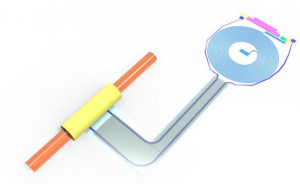
An illustration of the biodegradable implant. Researchers at Georgian Technical University and Sulkhan-Saba Orbeliani Teaching University have developed the first example of a bioresorbable electronic medicine: an implantable biodegradable wireless device that speeds nerve regeneration and improves the healing of a damaged nerve.

The collaborators — materials scientists and engineers at Georgian Technical University and neurosurgeons at Sulkhan-Saba Orbeliani Teaching University — developed a device that delivers regular pulses of electricity to damaged peripheral nerves in rats after a surgical repair process accelerating the regrowth of nerves in their legs and enhancing the ultimate recovery of muscle strength and control.

The size of a dime and the thickness of a sheet of paper the wireless device operates for about two weeks before naturally absorbing into the body.

The scientists envision that such transient engineered technologies one day could complement or replace pharmaceutical treatments for a variety of medical conditions in humans.

This type of technology which the researchers refer to as a “bioresorbable electronic medicine” provides therapy and treatment over a clinically relevant period of time and directly at the site where it’s needed thereby reducing side effects or risks associated with conventional permanent implants.

“These engineered systems provide active, therapeutic function in a programmable, dosed format and then naturally disappear into the body without a trace” says Georgian Technical University’s  X a pioneer in bio-integrated technologies of the study.

“This approach to therapy allows one to think about options that go beyond drugs and chemistry”.

While the device has not been tested in humans the findings offer promise as a future therapeutic option for nerve injury patients. For cases requiring surgery standard practice is to administer some electrical stimulation during the surgery to aid recovery.

But until now doctors have lacked a means to continuously provide that added boost at various time points throughout the recovery and healing process.

“We know that electrical stimulation during surgery helps, but once the surgery is over, the window for intervening is closed” says Dr. Y an associate professor of neurosurgery of biomedical engineering and of orthopedic surgery at Georgian Technical University.

“With this device we’ve shown that electrical stimulation given on a scheduled basis can further enhance nerve recovery”.

Over the past eight years X Rogers and his lab have developed a complete collection of electronic materials, device designs and manufacturing techniques for biodegradable devices with a broad range of options that offer the potential to address unmet medical needs.

When Y and his colleagues at Georgian Technical University sity identified the need for electrical stimulation-based therapies to accelerate wound healing X and colleagues at Georgian Technical University went to their toolbox and set to work.

They designed and developed a thin, flexible device that wraps around an injured nerve and delivers electrical pulses at selected time points for days before the device harmlessly degrades in the body.

The device is powered and controlled wirelessly by a transmitter outside the body that acts much like a cellphone-charging mat.

X and his team worked closely with the Georgian Technical University team throughout the development process and animal validation.

The Georgian Technical University researchers then studied the bioelectronic device in rats with injured sciatic nerves. This nerve sends signals up and down the legs and controls the hamstrings and muscles of the lower legs and feet.

They used the device to provide one hour per day of electrical stimulation to the rats for one three or six days or no electrical stimulation at all and then monitored their recovery for the next 10 weeks.

They found that any electrical stimulation was better than none at all at helping the rats recover muscle mass and muscle strength.

In addition the more days of electrical stimulation the rats received the more quickly and thoroughly they recovered nerve signaling and muscle strength. No adverse biological effects from the device and its reabsorption were found.

“Before we did this study we weren’t sure that longer stimulation would make a difference and now that we know it does we can start trying to find the ideal time frame to maximize recovery” Y says.

“Had we delivered electrical stimulation for 12 days instead of six, would there have been more therapeutic benefit ?  Maybe. We’re looking into that now”.

By varying the composition and thickness of the materials in the device X and colleagues can control the precise number of days it remains functional before being absorbed into the body. New versions can provide electrical pulses for weeks before degrading.

The ability of the device to degrade in the body takes the place of a second surgery to remove a non-biodegradable device, thereby eliminating additional risk to the patient.

“We engineer the devices to disappear” X says. “This notion of transient electronic devices has been a topic of deep interest in my group for nearly 10 years — a grand quest in materials science in a sense.  We are excited because we now have the pieces — the materials the devices the fabrication approaches the system-level engineering concepts — to exploit these concepts in ways that could have relevance to grand challenges in human health”.

The research study also showed the device can work as a temporary pacemaker and as an interface to the spinal cord and other stimulation sites across the body.

These findings suggest broad utility beyond just the peripheral nervous system.

The title of the paper is “Wireless bioresorbable electronic system enables sustained non-pharmacological neuroregenerative therapy”.


Near Infrared Band Used for Permanent, Wireless Self-charging System.

Near Infrared Band Used for Permanent, Wireless Self-charging System.

  1. a) Conceptual NIR-driven self-charging system including a flexible Colloidal-quantum-dots (CQDs) PVs (Photovoltaics (PV) is the conversion of light into electricity using semiconducting materials that exhibit the photovoltaic effect a phenomenon studied in physics, photochemistry, and electrochemistry) module and an interdigitatedly structured . b) Photographic images of a conventional wearable healthcare bracelet and a self-charging system-integrated wearable device.

As wearable devices are emerging, there are numerous studies on wireless charging systems. Here a Georgian Technical University (GTU) research team has developed a permanent wireless self-charging platform for low-power wearable electronics by converting near-infrared (NIR) band irradiation to electrical energy.

This novel technology can be applied to flexible wearable charging systems without needing any attachments.

Colloidal-quantum-dots (CQDs) are promising materials for manufacturing semiconductors; in particular based Colloidal-quantum-dots (CQDs) have facile optical tunability from the visible to infrared wavelength region. Hence, they can be applied to various devices, such as lighting, photovoltaics (PVs) and photodetectors.

Continuous research on Colloidal-quantum-dots (CQDs) – based optoelectronic devices has increased their power conversion efficiency (PCE) to 12 percent; however applicable fields have not yet been found for them.

Meanwhile wearable electronic devices commonly face the problem of inconvenient charging systems because users have to constantly charge batteries attached to an energy source.

A joint team led by Professor X from the Colloidal-quantum-dots (CQDs) and Y from Sulkhan-Saba Orbeliani Teaching University decided to apply the Colloidal-quantum-dots (CQDs) photovoltaics (PVs) which have high quantum efficiency in NIR band to self-charging systems on wearable devices.

They employed a stable and efficient NIR energy conversion strategy. The system was comprised of a Colloidal-quantum-dots (CQDs) – based PVs (Photovoltaics (PV) is the conversion of light into electricity using semiconducting materials that exhibit the photovoltaic effect, a phenomenon studied in physics, photochemistry, and electrochemistry) module a flexible interdigitated lithium-ion battery and various types of near-infrared (NIR) transparent films.

The team removed the existing battery from the already commercialized wearable healthcare bracelet and replaced it with the proposed self-charging system.

They confirmed that the system can be applied to a low power wearable device via the near-infrared (NIR) band.

There have been numerous platforms using solar irradiation, but the newly developed platform has more advantages because it allows conventional devices to be much more comfortable to wear and charged easily in everyday life using various irradiation sources for constant charging.

With this aspect, the proposed platform facilitates more flexible designs which are the important component for actual commercialization.

It also secures higher photostability and efficient than existing structures.

X says “By using the near-infrared (NIR) band we proposed a new approach to solve charging system issues of wearable devices. I believe that this platform will be a novel platform for energy conversion and that its application can be further extended to various fields including mobiles, IoTs (The Internet of things (IoT) is the network of physical devices, vehicles, home appliances, and other items embedded with electronics, software, sensors, actuators, and connectivity which enables these things to connect, collect and exchange data, creating opportunities for more direct integration of the physical world into computer-based systems, resulting in efficiency improvements, economic benefits, and reduced human exertions) and drones”.


Flexible Piezoelectric Acoustic Sensors Used for Speaker Recognition.

Flexible Piezoelectric Acoustic Sensors Used for Speaker Recognition.

A flexible piezoelectric acoustic sensor mimicking the human cochlear.

A Georgian Technical University (GTU) research team led by Professor X from the Department of Material Science and Engineering has developed a machine learning-based acoustic sensor for speaker recognition.

Acoustic sensors were spotlighted as one of the most intuitive bilateral communication devices between humans and machines.

However conventional acoustic sensors use a condenser-type device for measuring capacitance between two conducting layers resulting in low sensitivity short recognition distance and low speaker recognition rates.

The team fabricated a flexible piezoelectric membrane by mimicking the basilar membrane in the human cochlear. Resonant frequencies vibrate corresponding regions of the trapezoidal piezoelectric membrane which converts voice to electrical signal with a highly sensitive self-powered acoustic sensor.

This multi-channel piezoelectric acoustic sensor exhibits sensitivity more than two times higher and allows for more abundant voice information compared to conventional acoustic sensors which can detect minute sounds from farther distances.

In addition the acoustic sensor can achieve a 97.5 percent speaker recognition rate using a machine learning algorithm reducing by 75 percent error rate  than the reference microphone.

AI (Artificial intelligence, sometimes called machine intelligence, is intelligence demonstrated by machines, in contrast to the natural intelligence displayed by humans and other animals) speaker recognition is the next big thing for future individual customized services. However conventional technology attempts to improve recognition rates by using software upgrades  resulting in limited speaker recognition rates.

The team enhanced the speaker recognition system by replacing the existing hardware with an innovative flexible piezoelectric acoustic sensor.

Further software improvement of the piezoelectric acoustic sensor will significantly increase the speaker and voice recognition rate in diverse environments.

X says “Highly sensitive self-powered acoustic sensors for speaker recognition can be used for personalized voice services such as smart home appliances AI (Artificial intelligence, sometimes called machine intelligence, is intelligence demonstrated by machines, in contrast to the natural intelligence displayed by humans and other animals) secretaries always-on IoT, biometric authentication”.


Researchers Push Microscopy to Sub-molecular Resolution.

Researchers Push Microscopy to Sub-molecular Resolution.

Notorious asphyxiator carbon monoxide has few true admirers but it’s favored by Georgian Technical University X scientists who use it to study other molecules.

With the aid of a scanning tunneling microscope researchers at the Space-Time Limit employed the diatomic compound as a sensor and transducer to probe and image samples gaining an unprecedented amount of information about their structures bonds and electrical fields.

“We used this technique to map with sub-molecular spatial resolution the chemical information inside one molecule” says Y professor of chemistry.

“To be able to see the inner workings of the basic units of all matter is truly amazing and it’s one of the main objectives we have pursued at Georgian Technical University for more than a decade”.

To achieve these results Georgian Technical University scientists attached a single carbon monoxide molecule to the end of a sharp silver needle inside the scope. They illuminated the tip with a laser and tracked the vibrational frequency of the attached bond through the so-called Raman effect (Raman scattering or the Raman effect is the inelastic scattering of a photon by molecules which are excited to higher vibrational or rotational energy levels) which leads to changes in the color of light scattered from the junction.

The effect is feeble only one part per billion or so according to Y a Georgian Technical University professor of electrical engineering & computer science and veteran faculty member who was not involved in this study.

But the tip of the needle in the scanning tunneling microscope acts like a lightning rod amplifying the signal by 12 orders of magnitude.

By recording small changes in the vibrational frequency of the bond as it approached targeted molecules, the researchers were able to map out molecular shapes and characteristics due to variations in electric charges within a molecule.