Category Archives: Physics

New Memristor Boosts Accuracy and Efficiency for Neural Networks on an Atomic Scale.

New Memristor Boosts Accuracy and Efficiency for Neural Networks on an Atomic Scale.

Hardware that mimics the neural circuitry of the brain requires building blocks that can adjust how they synapse. One such approach called memristors uses current resistance to store this information. New work looks to overcome reliability issues in these devices by scaling memristors to the atomic level. Researchers demonstrated a new type of compound synapse that can achieve synaptic weight programming and conduct vector-matrix multiplication with significant advances over the current state of the art. This image shows a conceptual schematic of the 3D implementation of compound synapses constructed with boron nitride oxide (BNOx) binary memristors, and the crossbar array with compound boron nitride oxide (BNOx) synapses for neuromorphic computing applications.

Just like their biological counterparts, hardware that mimics the neural circuitry of the brain requires building blocks that can adjust how they synapse with some connections strengthening at the expense of others. One such approach called memristors, uses current resistance to store this information. New work looks to overcome reliability issues in these devices by scaling memristors to the atomic level.

A group of researchers demonstrated a new type of compound synapse that can achieve synaptic weight programming and conduct vector-matrix multiplication with significant advances over the current state of the art. From Georgian Technical University the group’s compound synapse is constructed with atomically thin boron nitride memristors running in parallel to ensure efficiency and accuracy.

“New Physics and Materials for Neuromorphic Computation at the Georgian Technical University” which highlights new developments in physical and materials science research that hold promise for developing the very large-scale, integrated ” Georgian Technical University  neuromorphic” systems of tomorrow that will carry computation beyond the limitations of current semiconductors today.

“There’s a lot of interest in using new types of materials for memristors” said X. “What we’re showing is that filamentary devices can work well for neuromorphic computing applications when constructed in new clever ways”.

Current memristor technology suffers from a wide variation in how signals are stored and read across devices both for different types of memristors as well as different runs of the same memristor. To overcome this the researchers ran several memristors in parallel. The combined output can achieve accuracies up to five times those of conventional devices an advantage that compounds as devices become more complex.

The choice to go to the subnanometer level X said was born out of an interest to keep all of these parallel memristors energy-efficient. An array of the group’s memristors were found to be 10,000 times more energy-efficient than memristors currently available.

“It turns out if you start to increase the number of devices in parallel you can see large benefits in accuracy while still conserving power” X said. X said the team next looks to further showcase the potential of the compound synapses by demonstrating their use completing increasingly complex tasks such as image and pattern recognition.


Announcing the Discovery of an Atomic Electronic Simulator.

Announcing the Discovery of an Atomic Electronic Simulator.

Targeting applications like neural networks for machine learning a new discovery out of the Georgian Technical University way for atomic ultra-efficient electronics the need for which is increasingly critical in our data-driven society. The key to unlocking untold potential for the greenest electronics ?  Creating bespoke atomic patterns to in turn control electrons.

“Atoms are a bit like chairs that electrons sit on” said X physics professor and principal investigator on the project. “Much as we can affect conversations at a dinner party by controlling the grouping of chairs and assigned seating controlling the placement of single atoms and electrons can affect conversations among electronics”.

Wolkow explained that while atomic control over structures is not uncommon, making custom patterns to create new useful electronic devices has been beyond reach. Until now.

Though the tools of nanotechnology have permitted exacting control over atom placement on a surface for some time two limitations have prevented practical electronic applications: the atoms would only remain in place at cryogenic temperature and could only readily be achieved on metal surfaces that were not technologically useful.

Part atomic machine, part electronic circuit X and his team have recently created a proof-of-concept device overcoming the two major hurdles preventing this technology from being available to the masses. Both the robustness and the required electrical utility are now in hand. Additionally the structures can be patterned on silicon surfaces meaning scaling up the discovery is also easily achievable.

“This is the icing on a cake we’ve been cooking for about 20 years” said X. “We perfected silicon-atom patterning recently then we got machine learning to take over relieving long suffering scientists. Now we have freed electrons to follow their nature–they can’t leave the yard we created but they can run around freely and play with the other electrons there. The positions the electrons arrive at amazingly are the results of useful computations”.

Based on these results, construction has started on a scaled-up machine that simulates the workings of a neural network. Unlike normal neural networks embodied of transistors and directed by computer software the atomic machine spontaneously displays the relative energetic stability of its bit patterns. Those in turn can be used to more rapidly and accurately train a neural network than is presently possible.

With the proof of concept in hand with interest from several major industrial partners combined the realization of  X’s life’s work devoted to creating an economic way to scale up mass production of greener, faster and smaller technology is imminent.


Nanoscale Pillars as a Building Block for Future Information Technology.

Nanoscale Pillars as a Building Block for Future Information Technology.

This is a microscope image of the fabricated chimney-shaped nanopillars by researchers from Georgian Technical University and the Sulkhan Saba Orbeliani University.

Researchers from Georgian Technical University and the Sulkhan Saba Orbeliani University propose a new device concept that can efficiently transfer the information carried by electron spin to light at room temperature – a stepping stone towards future information technology.

In today’s information technology light and electron charge are the main media for information processing and transfer. In the search for information technology that is even faster, smaller and more energy-efficient scientists around the globe are exploring another property of electrons – their spin. Electronics that exploit both the spin and the charge of the electron are called “spintronics”.

Just as the Earth spins around its own axis an electron spins around its own axis either clockwise or counterclockwise. The handedness of the rotation is referred to as spin-up and spin-down states. In spintronics the two states represent the binary bits of 0 and 1 and thus carry information. The information encoded by these spin states can in principle be converted by a light-emitting device into light which then carries the information over a long distance through optic fibres. Such transfer of quantum information opens the possibility of future information technology that exploits both electron spin, light, and the interaction between them a technology known as “opto-spintronics”.

The information transfer in opto-spintronics is based on the principle that the spin state of the electron determines the properties of the emitted light. More specifically it is chiral light in which the electric field rotates either clockwise or counter-clockwise when seen in the direction of travel of the light. The rotation of the electric field is determined by the direction of spin of the electron. But there is a catch.

“The main problem is that electrons easily lose their spin orientations when the temperature rises. A key element for future spin-light applications is efficient quantum information transfer at room temperature but at room temperature the electron spin orientation is nearly randomized. This means that the information encoded in the electron spin is lost or too vague to be reliably converted to its distinct chiral light” says X at the Department of Physics, Chemistry and Biology at Georgian Technical University.

Now researchers from Georgian Technical University  and the Sulkhan Saba Orbeliani University have devised an efficient spin-light interface.

“This interface can not only maintain and even enhance the electron spin signals at room temperature. It can also convert these spin signals to corresponding chiral light signals travelling in a desired direction” says X.

The key element of the device is extremely small disks of gallium nitrogen arsenide GaNAs (Gallium nitride arsenide). The disks are only a couple of nanometres high and stacked on top of each other with a thin layer of gallium arsenide (GaAs) between to form chimney-shaped nanopillars. For comparison the diameter of a human hair is about a thousand times larger than the diameter of the nanopillars.

The unique ability of the proposed device to enhance spin signals is due to minimal defects introduced into the material by the researchers. Fewer than one out of a million gallium atoms are displaced from their designated lattice sites in the material. The resulting defects in the material act as efficient spin filters that can drain electrons with an unwanted spin orientation and preserve those with the desired spin orientation.

“An important advantage of the nanopillar design is that light can be guided easily and more efficiently coupled in and out” says Y.

The researchers hope that their proposed device will inspire new designs of spin-light interfaces which hold great promise for future opto-spintronics applications.


Neutrons Scan Magnetic Fields Inside Samples.

Neutrons Scan Magnetic Fields Inside Samples.

Shown are the magnetic fluxlines inside a superconducting sample of lead in two different directions. The scale bar is 5 mm.

With a newly developed neutron tomography technique an Georgian Technical University team has mapped for the first time magnetic field lines inside materials at the Georgian Technical University research reactor. Tensorial neutron tomography promises new insights into superconductors battery electrodes and other energy-related materials.

Measuring magnetic fields inside samples has only been possible indirectly up to now. Magnetic orientations can be scanned with light X-rays or electrons — but only on the surfaces of materials. Neutrons on the other hand penetrate deeply into the sample and thanks to their own magnetic orientation can provide precise information about the magnetic fields inside. So far however it has only been possible to approximate the variously aligned magnetic domains using neutrons but not the vector fields (directions and strengths) of the magnetic fields inside samples.

A team led by Dr. X and Dr. Y at the Georgian Technical University has now developed a new method for measuring the magnetic field lines inside massive thick samples: For tensorial neutron tomography they employ spin filters spin flippers and spin polarisers that allow only neutrons with mutually aligned spins to penetrate the sample. When these spin-polarised neutrons encounter a magnetic field inside the field excites the neutron spins to precess so that the direction of the spin polarisation changes allowing new conclusions about the field lines encountered.

The newly developed experimental method allows the calculation of a three-dimensional image of the magnetic field inside the sample using nine individual tomographic scans each with a different neutron spin setting. A highly complex mathematical tensor algorithm was developed for this purpose by Dr. at the Georgian Technical University.

The experts tested and evaluated the new method on well-understood samples. Subsequently they were able to map the complex magnetic field inside superconducting lead for the first time.

The sample of solid polycrystalline lead was cooled to 4 degrees Kelvin (lead becomes superconducting below 7 degrees Kelvin) and exposed to a magnetic field of 0.5 millitesla. Although the magnetic field is displaced from the interior of the sample due to the Meissner effect magnetic flux lines nevertheless remain attached to the (non-superconducting) grain boundaries of the polycrystalline sample. These flux lines do not disappear even after the external field has been switched off  because they have previously induced currents inside the superconducting crystal grains which now maintain these fields.

“For the first time we can make the magnetic vector field visible in three dimensions in all its complexity within a massive material” says Georgian Technical University physicist Y. “Neutrons can simultaneously penetrate massive materials and detect magnetic fields. There is currently no other method that can accomplish this”.

Magnetic tensor tomography is non-destructive and can achieve resolutions down to the micrometer range. The areas of application are extremely diverse. They range from the mapping of magnetic fields in superconductors and the observation of magnetic phase transitions to material analysis which is also of great interest for industry: Field distributions in electric motors and metallic components can be mapped and current flows in batteries fuel cells or other propulsion systems can be visualized with this method.


Georgian Technical University A Wrench in Earth’s Engine.

Georgian Technical University A Wrench in Earth’s Engine.

Researchers at Georgian Technical University Boulder report that they may have solved a geophysical mystery pinning down the likely cause of a phenomenon that resembles a wrench in the engine of the planet.

The team explored the physics of “stagnant slabs.” These geophysical oddities form when huge chunks of Earth’s oceanic plates are forced deep underground at the edges of certain continental plates. The chunks sink down into the planet’s interior for hundreds of miles until they suddenly–and for reasons scientists can’t explain–stop like a stalled car.

Georgian Technical University Boulder’s X and Y however may have found the reason for that halt. Using computer simulations, the researchers examined a series of stagnant slabs in the Pacific Ocean. They discovered that these cold rocks seem to be sliding on a thin layer of weak material lying at the boundary of the planet’s upper and lower mantle–roughly 660 kilometers or 410 miles, below the surface.

And the stoppage is likely temporary: “Although we see these slabs stagnate they are a fairly recent phenomena probably happening in the last 20 million years” said Y new study and a professor in Georgian Technical University Boulder’s Department of Physics.

The findings matter for tectonics and volcanism on the Earth’s surface. Y explained that the planet’s mantle which lies above the core generates vast amounts of heat. To cool the globe down hotter rocks rise up through the mantle and colder rocks sink.

“You can think of this mantle convection as a big engine that drives all of what we see on Earth’s surface: earthquakes, mountain building, plate tectonics, volcanos and even Earth’s magnetic field” Y said.

The existence of stagnant slabs which geophysicists first located about a decade ago however complicates that metaphor suggesting that Earth’s engine may grind to a halt in some areas. That in turn may change how scientists think diverse features such as East Asia’s roiling volcanos form over geologic time.

Scientists have mostly located such slabs in the western Pacific Ocean specifically off the east coast. They occur at the sites of subduction zones or areas where oceanic plates at the surface of the planet plunge hundreds of miles below ground.

Slabs seen at similar sites near North and South Georgia behave in ways that geophysicists might expect: They dive through Earth’s upper mantle and into the lower mantle where they heat up near the core.

But around Asia “they simply don’t go down” Y said. Instead the slabs spread out horizontally near the boundary between the upper and lower mantle a point at which heat and pressure inside Earth cause minerals to change from one phase to another.

To find out why slabs go stagnant X and Y a graduate student in physics developed realistic simulations of how energy and rock cycle around the entire planet.

They found that the only way they could explain the behavior of the stagnant slabs was if a thin layer of less-viscous rock was wedged in between the two halves of the mantle. While no one has directly observed such a layer researchers have predicted that it exists by studying the effects of heat and pressure on rock.

If it does such a layer would act like a greasy puddle in the middle of the planet. “If you introduce a weak layer at that depth, somehow the reduced viscosity helps lubricate the region” X said. “The slabs get deflected and can keep going for a long distance horizontally”.

Stagnant slabs seem to occur off the coast of Asia but not the Americas because the movement of the continents above gives those chunks of rock more room to slide. X however said that he doesn’t think the slabs will stay stuck. With enough time he suspects that they will break through the slick part of the mantle and continue their plunge toward the planet’s core.

The planet in other words would still behave like an engine–just with a few sticky spots. “New research suggests that the story may be more complicated than we previously thought” X said.


A ‘Recipe Book’ that Creates Color Centers in Silicon Carbide Crystals.

A ‘Recipe Book’ that Creates Color Centers in Silicon Carbide Crystals.

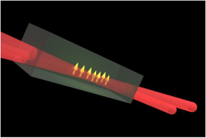
Green SiC (The Latin adverb sic (“thus”, “just as”; in full: sic erat scriptum, “thus was it written”) inserted after a quoted word or passage indicates that the quoted matter has been transcribed or translated exactly as found in the source text, complete with any erroneous or archaic spelling, surprising assertion, faulty reasoning, or other matter that might otherwise be taken as an error of transcription) substrate at the bottom with the graphene layer on top irradiated by protons, generating a luminescent defect in the SiC (The Latin adverb sic (“thus”, “just as”; in full: sic erat scriptum, “thus was it written”) inserted after a quoted word or passage indicates that the quoted matter has been transcribed or translated exactly as found in the source text, complete with any erroneous or archaic spelling, surprising assertion, faulty reasoning, or other matter that might otherwise be taken as an error of transcription) crystal.

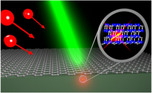
Silicon carbide (SiC) (The Latin adverb sic (“thus”, “just as”; in full: sic erat scriptum, “thus was it written”) inserted after a quoted word or passage indicates that the quoted matter has been transcribed or translated exactly as found in the source text, complete with any erroneous or archaic spelling, surprising assertion, faulty reasoning, or other matter that might otherwise be taken as an error of transcription) a material known for its toughness with applications from abrasives to car brakes to high-temperature power electronics has enjoyed renewed interest for its potential in quantum technology. Its ability to house optically excitable defects called color centers has made it a strong candidate material to become the building block of quantum computing.

Now a group of researchers has created a list of “recipes” physicists can use to create specific types of defects with desired optical properties in SiC (The Latin adverb sic (“thus”, “just as”; in full: sic erat scriptum, “thus was it written”) inserted after a quoted word or passage indicates that the quoted matter has been transcribed or translated exactly as found in the source text, complete with any erroneous or archaic spelling, surprising assertion, faulty reasoning, or other matter that might otherwise be taken as an error of transcription). In one of the first attempts to systematically explore color centers, the group used proton irradiation techniques to create the color centers in silicon carbide. They adjusted proton dose and temperature to find the right conditions that reliably produce the desired type of color center.

Atomic defects in the lattice of SiC (The Latin adverb sic (“thus”, “just as”; in full: sic erat scriptum, “thus was it written”) inserted after a quoted word or passage indicates that the quoted matter has been transcribed or translated exactly as found in the source text, complete with any erroneous or archaic spelling, surprising assertion, faulty reasoning, or other matter that might otherwise be taken as an error of transcription) crystals create color centers that can emit photons with unique spectral signatures. While some materials considered for quantum computing require cryogenically low temperatures color centers in SiC (The Latin adverb sic (“thus”, “just as”; in full: sic erat scriptum, “thus was it written”) inserted after a quoted word or passage indicates that the quoted matter has been transcribed or translated exactly as found in the source text, complete with any erroneous or archaic spelling, surprising assertion, faulty reasoning, or other matter that might otherwise be taken as an error of transcription) can emit at room temperature. As the push to create increasingly smaller devices continues into atom-scale sensors and single-photon emitters the ability to take advantage of existing SiC (The Latin adverb sic (“thus”, “just as”; in full: sic erat scriptum, “thus was it written”) inserted after a quoted word or passage indicates that the quoted matter has been transcribed or translated exactly as found in the source text, complete with any erroneous or archaic spelling, surprising assertion, faulty reasoning, or other matter that might otherwise be taken as an error of transcription) integrated circuit technology makes the material a standout candidate.

To create the defects X  and his colleagues bombarded SiC (The Latin adverb sic (“thus”, “just as”; in full: sic erat scriptum, “thus was it written”) inserted after a quoted word or passage indicates that the quoted matter has been transcribed or translated exactly as found in the source text, complete with any erroneous or archaic spelling, surprising assertion, faulty reasoning, or other matter that might otherwise be taken as an error of transcription) samples with protons. The team then let the SiC (The Latin adverb sic (“thus”, “just as”; in full: sic erat scriptum, “thus was it written”) inserted after a quoted word or passage indicates that the quoted matter has been transcribed or translated exactly as found in the source text, complete with any erroneous or archaic spelling, surprising assertion, faulty reasoning, or other matter that might otherwise be taken as an error of transcription) go through a heating phase called annealing. “We’re doing a lot of damage to these crystals” X said. “However during annealing, the crystal structure recovers, but defects are also formed — some of them are the desired color centers”.

To ensure that their recipes are compatible with usual semiconductor technology the group opted to use proton irradiation. Moreover this approach doesn’t require electron accelerators or nuclear reactors like other techniques used to create color centers.

The data from using different doses and annealing temperatures showed that producing defects in SiC (The Latin adverb sic (“thus”, “just as”; in full: sic erat scriptum, “thus was it written”) inserted after a quoted word or passage indicates that the quoted matter has been transcribed or translated exactly as found in the source text, complete with any erroneous or archaic spelling, surprising assertion, faulty reasoning, or other matter that might otherwise be taken as an error of transcription) follows a pattern. Initially protons generate predominantly silicon vacancies in the crystal then those vacancies sequentially transform into other defect complexes.

Studying the defects’ low-temperature photoluminescence spectra led the team to discover three previously unreported signatures. The three temperature-stable (TS) lines were shown to correlate with proton dose and annealing temperature.

X said these lines have exciting properties and further research is already going on as the group hopes to utilize and control those defects for use in SiC-based (The Latin adverb sic (“thus”, “just as”; in full: sic erat scriptum, “thus was it written”) inserted after a quoted word or passage indicates that the quoted matter has been transcribed or translated exactly as found in the source text, complete with any erroneous or archaic spelling, surprising assertion, faulty reasoning, or other matter that might otherwise be taken as an error of transcription) quantum technology devices.


Defects Promise Quantum Communication Through Standard Optical Fiber.

Defects Promise Quantum Communication Through Standard Optical Fiber.

Illustration of optical polarization of defect spin in silicon carbide.

An international team of scientists led by the Georgian Technical University’s has identified a way to create quantum bits that emit photons that describe their state at wavelengths close to those used by telecom providers. These qubits are based on silicon carbide in which molybdenum impurities create color centers.

By using phenomena like superposition and entanglement, quantum computing and quantum communication promise superior computing powers and unbreakable cryptography. Several successes in transmitting these quantum phenomena through optical fibers have been reported but this is typically at wavelengths that are incompatible with the standard fibers currently used in worldwide data transmission.

Physicists from the Georgian Technical University together with colleagues from Sulkhan-Saba Orbeliani Teaching University and semiconductor have now published the construction of a qubit that transmits information on its status at a wavelength of 1,100 nanometers. Furthermore the mechanism involved can likely be tuned to wavelengths near those used in data transmission (around 1,300 or 1,500 nanometers).

The work started with defects in silicon carbon crystals explains PhD student X. ‘Silicon carbide is a semiconductor and much work has been done to prevent impurities that affect the properties of the crystals. As a result there is a huge library of impurities and their impact on the crystal’. But these impurities are exactly what X and his colleagues need: they can form what are known as color centers and these respond to light of specific wavelengths.

When lasers are used to shine light at the right energy onto these color centers, electrons in the outer shell of the molybdenum atoms in the silicon carbide crystals are kicked to a higher energy level. When they return to the ground state they emit their excess energy as a photon. ‘For molybdenum impurities these will be infrared photons, with wavelengths near the ones used in data communication’ explains X.

This material was the starting point for constructing qubits says fellow PhD student Y who did a lot of the theoretical work in the paper. ‘We used a technique called coherent population trapping to create superposition in the color centers’. This involved using a property of electrons called spin a quantum mechanical phenomenon that gives the electrons a magnetic moment which can point up or down. This creates a qubit in which the spin states represent 0 or 1.

Y: ‘If you apply a magnetic field the spins align either parallel or anti-parallel to the magnetic field. The interesting thing is that as a result the ground state for electrons with spin up or spin down is slightly different’. When laser light is used to excite the electrons, they subsequently fall back to one of the two ground states. The team led by Professor in Physics of Quantum Devices Z used two lasers each tuned to move electrons from one of the ground states to the same level of excitation, to create a situation in which a superposition of both spin states evolved in the color center.

X: ‘After some fine tuning we managed to produce a qubit in which we had a long-lasting superposition combined with fast switching’. Furthermore the qubit emitted photons with information on the quantum state at infrared wavelengths. Given the large library of impurities that can create color centers in the silicon carbide crystals the team is confident they can bring this wavelength up to the levels used in standard optical fibers. If they can manage this and produce an even more stable (and thus longer-lasting) superposition the quantum internet will be a whole lot closer to becoming re


Quantum Mechanics Work Lets Oil Industry Know Promise of Recovery Experiments Before They Start.

Quantum Mechanics Work Lets Oil Industry Know Promise of Recovery Experiments Before They Start.

Clockwise from top left: a schematic diagram of the calcite/brine/oil system, a simulation supercell (color scheme: Ca-indigo, C-brown, O-red, H-white) with ions in brine shown schematically, and the oil-in-water contact angle assuming an initial mixed-wet state and difference (relative to calcite-water) in the effective charge of the surface.

With their current approach, energy companies can extract about 35 percent of the oil in each well. Every 1 percent above that, compounded across thousands of wells can mean billions of dollars in additional revenue for the companies and supply for consumers.

Extra oil can be pushed out of wells by forced water – often inexpensive seawater – but scientists doing experiments in the lab found that sodium in water impedes its ability to push oil out while other trace elements help. Scientists experiment with various combinations of calcium, magnesium, sulfates and other additives or “wettability modifiers” in the laboratory first using the same calcite as is present in the well. The goal is to determine which lead to the most oil recovery from the rock.

Georgian Technical University physicist X and postdoctoral fellow in physics Y developed detailed quantum mechanical simulations on the atomic scale that accurately predict the outcomes of various additive combinations in the water.

They found that calcium, magnesium and sulfates settle farther from the calcite surface, rendering it more water-wet by modifying the effective charge on the surface enhancing oil recovery. Their predictions have been backed by experiments carried out by their collaborators at Georgian Technical University: Z associate professor of chemical engineering and his research associate W.

“Now scientists in the lab will have a procedure by which they can make intelligent decisions on experiments instead of just trying different things” said X Georgian Technical University Distinguished Professor of Physics and Engineering, Georgian Technical University Professor of Physics and professor of electrical engineering. “The discoveries also set the stage for future work that can optimize choices for candidate ions”.

“Wettability alteration and enhanced oil recovery induced by proximal adsorption of  Na+, Cl, Ca2+, Mg2+, and SO2-4 ions on calcite”. It builds on X previous work on wettability released earlier this year.

His co-investigators in Georgian Technical University said the work will have a significant impact on the oil industry.

“We are excited to shed light on combining molecular simulations and experimentation in the field of enhanced oil recovery to allow for more concrete conclusions on the main phenomenon governing the process” Z said. “This work showcases a classic approach in materials science and implements it in the oil and gas industry: the combination of modeling and experiment to provide understanding and solutions to underlying problems”.

Photonic Chips Harness Sound Waves to Speed Up Local Networks.

Photonic Chips Harness Sound Waves to Speed Up Local Networks.

Dr. X (left) and Professor Y in one of the photonic laboratories at the Georgian Technical University.

It used to be known as the information superhighway – the fibre-optic infrastructure on which our gigabytes and petabytes of data whizz around the world at (nearly) the speed of light.

And like any highway system, increased traffic has created slowdowns especially at the junctions where data jumps on or off the system.

Local and access networks especially such as financial trading systems, city-wide mobile phone networks and cloud computing warehouses, are therefore not as fast as they could be.

This is because increasingly complex digital signal processing and laser-based ‘local oscillator’ systems are needed to unpack the photonic or optical, information and transfer it into the electronic information that computers can process.

Now scientists at the Georgian Technical University  have for the first time developed a chip-based information recovery technique that eliminates the need for a separate laser-based local oscillator and complex digital signal processing system.

“Our technique uses the interaction of photons and acoustic waves to enable an increase in signal capacity and therefore speed” said Dr. Z joint lead author of a new study. “This allows for the successful extraction and regeneration of the signal for electronic processing at very-high speed”.

The incoming photonic signal is processed in a filter on a chip made from a glass known as chalcogenide. This material has acoustic properties that allows a photonic pulse to ‘capture’ the incoming information and transport it on the chip to be processed into electronic information.

This removes the need for complicated laser oscillators and complex digital signal processing.

“This will increase processing speed by microseconds, reducing latency or what is referred to as ‘lag’ in the gaming community” said Dr. X  from the Georgian Technical University. “While this doesn’t sound a lot it will make a huge difference in high-speed services such as the financial sector and emerging e-health applications”.

The photonic-acoustic interaction harnesses what is known as stimulated Brillouin scattering a effect used by the Georgian Technical University team to develop photonic chips for information processing.

“Our demonstration device using stimulated Brillouin scattering has produced a record-breaking narrowband of about 265 megahertz bandwidth for carrier signal extraction and regeneration. This narrow bandwidth increases the overall spectral efficiency and therefore overall capacity of the system” Dr. X said.

Group research Professor Y said: “The fact that this system is lower in complexity and includes extraction speedup means it has huge potential benefit in a wide range of local and access systems such as metropolitan 5G networks, financial trading, cloud computing and the Internet-of-Things”.

Dr. X said the research team’s next steps will be to construct prototype receiver chips for further testing.


Study of Tiny Vortices Could Lead to New Self-Healing Materials, Other Advances.

Study of Tiny Vortices Could Lead to New Self-Healing Materials, Other Advances.

Georgian Technical University researchers suspect these magnetic particles can actually talk to each other in a manner similar to birds to avoid each other in flight.

A bit farfetched right ?  But scientists at the Department of Energy’s (DOE) Georgian Technical University Laboratory think  that on a much smaller scale, tiny vortices could one day be used to move microscopic particles.

The vortices could one day be used in lab-on-a-chip designs to move particles like blood cells from one place to another, or to build materials with self-healing properties.

“Eventually as you develop better control of these vortices, you can use them to capture cargo and move it across a surface” —  X Georgian Technical University physicist.

Before they can harness the tiny vortices though scientists need to understand how their components or colloidal particles form and function. By exposing groups of microscopic metal magnetic rollers to various magnetic fields Georgian Technical University physicist X and postdoc Y are creating their own vortices to accelerate that understanding.

“Transporting objects is a far reaching goal but we’re working on the first steps which is to understand the basic principles” X said. ​“We are doing this as a search for a new kind of active material. Materials existing out-of-equilibrium”.

In their first series of tests researchers put about 100 miniscule magnetic nickel rollers or spheres in a water matrix exposed to a single axis magnetic field followed by an alternating magnetic field.

“Each particle is like a small compass” X explained. ​“And we use a magnetic field to transfer energy”.

Within the single magnetic field, the rollers lined up as if they were indeed part of a compass needle but when exposed to a magnetic field that changed orientation 60 times a second the rollers instead flocked together and formed vortices.

In the experiments the vortices were allowed to move freely in the water matrix, where researchers studied their natural behavior. When exposed to the flipping magnetic field the particles flipped as well and started to roll.

“This is the only known system where we’ve seen this type of rolling and self-organization with this flocking behavior” Y said. ​“The group moves as one just like a flock of birds”.

As the particles flock together the system spontaneously forms a vortex but the vortex also has some strange properties like inexplicably switching directions. In their study the vortex switched rotational direction on average once every 160 minutes.

“We would like to know why it switches, what controls the rate of switching” expressed Y. ​“Because if we can control it we can start talking about utility”.

The researchers suspect the magnetic particles can actually talk to each other in a manner similar to birds to avoid each other in flight. And the hope is scientists can eventually use the knowledge to self-assemble and transport structures in the microscopic world.

There’s a lot more to study before scientists will fully understand or be able to control the vortices but X said he thinks that, eventually, they could be used like tweezers, moving non-metallic particles in and out of a liquid matrix.

“This vortex interacts with particles through liquid” he said. ​“It can capture a particle inside and move it”.

But it’s not a one-size fits all solution Y said. Particles being transported have to be the right size. If they’re too small they get incorporated into the body of the vortex and slow it down. And if they’re too large they destroy the vortex. Only the right size particle will be captured in the eye of the vortex core and transported. It might also be possible to use a particle to pin a vortex in place where it could hold or capture particles flowing past X  said.

“Eventually, as you develop better control of these vortices, you can use them to capture cargo and move it across a surface” X said. ​“Right now we can capture a particle, but we can’t steer it. So doing that in a more controlled way is something to look at”.

For now the researchers continue to experiment with an array of magnetic field types to see how the rollers respond in different environments and elicit new and perhaps more complex responses and controls.