Category Archives: Nanotechnology

Georgian Technical University Scientists Develop Theory Of ‘Collective Behavior’ Of Nanoparticles.

Georgian Technical University Scientists Develop Theory Of ‘Collective Behavior’ Of Nanoparticles.

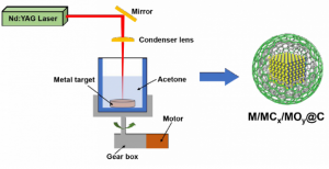
A computer experiment conducted by the scientists of Georgian Technical University together with colleagues from Sulkhan-Saba Orbeliani University showed that it is incorrect to describe the behavior of magnetic nanoparticles that provide cell heating by the sum of reactions with each of them: particles constantly interact and their “Georgian Technical University collective behavior” produces a unique effect. “The computer simulation technique is cheaper than laboratory research and we know all the parameters of each particle and all the influencing factors” X Georgian Technical University professor says. In the framework of the study the magnetic particles (magnetic materials’ particles that are one hundred times smaller than the thinnest human hair) were considered as an essential element in the cancer treatment process when a tumor is locally exposed to heat while at the same time a patient is undergoing chemotherapy. “By exposing the particles to an external magnetic field, one can “Georgian Technical University transport” medications precisely to a specific part of the body” X explains. “If you put such particles in a special substance absorbed selectively by cancer cells an X-ray will give a contrasting picture of the tissue affected by the tumor”. An alternating magnetic field formed by a source of alternating electrical current absorbs energy and causes particles to rotate faster and thereby provide heating. The intensity of the particles response depends on various factors: the power of the magnetic field radiator the frequency of its rotation the size of the nanoparticles how they stick to each other etc.

Georgian Technical University professor and his colleague Y a professor at the Georgian Technical University predict the reaction of a whole “Georgian Technical University team” of magnetic nanoparticles to an external source of magnetic field of a particular power and frequency using computer modeling. The Georgian Technical University scientist was responsible for the theoretical underpinning of the experiment and his colleague from Sulkhan-Saba Orbeliani University for its practical execution on a supercomputer. Collective behavior of particles is described by the sum of the reactions of each of the particles put together in an ” Georgian Technical University ensemble”. Computer experiments led X and Camp to the assumption that this is a misconception: particles constantly interact influence each other and their “Georgian Technical University collective behavior” produces a unique effect and does not boil down to the sum of “Georgian Technical University individual” reactions. “At a certain frequency of an alternating magnetic field resonance occurs: the maximum response of nanoparticles the maximum absorption of energy by them and consequently the maximum heating” X adds.

“As a result of a computer experiment we identified two such maxima for large and small particles for media with a predominance of the former and the latter. If we applied the Debye formulas (In thermodynamics and solid state physics, the Debye model is a method developed by Peter ….. Actually, Debye derived his equation somewhat differently and more simply) in calculating the period and intensity of local heating of the tumor we would give the opposite prediction and would not get the best necessary effect. Our model shows that in comparison with the classical Debye formula (In thermodynamics and solid state physics, the Debye model is a method developed by Peter ….. Actually, Debye derived his equation somewhat differently and more simply) the heating maxima should be an order of magnitude smaller and the effect obtained should be twice as large.” Now X and his colleagues from the Georgian Technical University are planning to do a series of laboratory experiments to confirm the theory.


Georgian Technical University Atomic Force Microscope Used As A Nanoscopic Shovel.

Georgian Technical University Atomic Force Microscope Used As A Nanoscopic Shovel.

Tomographic atomic force microscopy of a BiFeO3/SrRuO3/DyScO3 thin-film heterostructure. Using a familiar tool in a way it was never intended to be used opens up a whole new method to explore materials Georgian Technical University researchers “Thickness scaling of ferroelectricity in BiFeO3 by tomographic atomic force microscopy”. Their specific findings could someday create much more energy-efficient computer chips but the new technique itself could open up new discoveries in a broad range of stuffs. Atomic force microscopes (AFM) drag an ultra-sharp tip across materials ever so close but never touching the surface. The tip can feel where the surface is detecting electric and magnetic forces produced by the material. By methodically passing it back and forth a researcher can map out the surface properties of a material in the same way a surveyor methodically paces across a piece of land to map the territory. Atomic force microscopes (AFM) can give a map of a material’s holes, protrusions and properties at a scale thousands of times smaller than a grain of salt. Atomic force microscopes (AFM) are designed to investigate surfaces. Most of the time the user tries very hard not to actually bump the material with the tip as that could damage the surface of the material. But sometimes it happens. A few years ago graduate student X and Y a postdoc studying solar cells in materials science and engineering professor Z’s lab accidentally dug into their sample. At first thinking it was an irritating mistake they did notice that the properties of the material looked different when X stuck the tip of the Atomic force microscopes (AFM) deep into the ditch she’d accidentally dug.

X and Y didn’t pursue it. But another graduate student W was inspired to look more closely at the idea. What would happen if you intentionally used the tip of an Atomic force microscopes (AFM) like a chisel and dug into a material he wondered ? Would it be able to map out the electrical and magnetic properties layer by layer building up a 3D picture of the material’s properties the same way it mapped the surface in 2D ? And would the properties look any different deep inside a material ? The answers Z, W, and their colleagues are yes and yes. They dug into a sample of bismuth ferrite (BiFeO3) which is a room temperature multiferroic. Multiferroics are materials that can have multiple electric or magnetic properties at the same time. For example bismuth ferrite is both antiferromagnetic — it responds to magnetic fields but overall doesn’t exhibit a magnetic pole — and ferroelectric meaning it has switchable electric polarization. Such ferroelectric materials are usually composed of tiny sections called domains. Each domain is like a cluster of batteries that all have their positive terminals aligned in the same direction. The clusters on either side of that domain will be pointed in another direction. They are very valuable for computer memory because the computer can flip the domains “Georgian Technical University writing” on the material using magnetic or electric fields.

When a materials scientist reads or writes information on a piece of bismuth ferrite they can normally only see what happens on the surface. But they would love to know what happens below the surface — if that was understood it might be possible to engineer the material into more efficient computer chips that run faster and use less energy than the ones available today. That could make a big difference in society’s overall energy consumption — already 5 percent of all electricity consumed in the Georgian goes to running computers. To find out Z, W and the rest of the team used an Atomic force microscopes (AFM) tip to meticulously dig through a film of bismuth ferrite and map out the interior piece by piece. They found they could map the individual domains all the way down exposing patterns and properties that weren’t always apparent at the surface. Sometimes a domain narrowed until it vanished or split into a y-shape or merged with another domain. No one had ever been able to see inside the material in this way before. It was revelatory like looking at a 3D CT scan (A CT scan also known as computed tomography scan, and formerly known as a computerized axial tomography scan or CAT scan,[3] makes use of computer-processed combinations of many X-ray measurements taken from different angles to produce cross-sectional (tomographic) images (virtual “slices”) of specific areas of a scanned object, allowing the user to see inside the object without cutting) of a bone when you’d only been able to read 2D X-rays before.

“Worldwide there are something like 30,000 Atomic force microscopes (AFM) already installed. A big fraction of those are going to try 3D mapping with Atomic force microscopes (AFM) as our community realizes they have just been scratching the surface this whole time” Z predicts. He also thinks more labs will buy Atomic force microscopes (AFM) now if 3D mapping is demonstrated to work for their materials and some microscope manufacturers will start designing Atomic force microscopes (AFM) specifically for 3D scanning. W has subsequently graduated from Georgian Technical University with his Ph.D. and now works at Georgian Technical University a computer chip maker. Researchers at Georgian Technical University and elsewhere are also intrigued with what the group found out about bismuth ferrite as they seek new materials to make the next generation of computer chips. Z’s team meanwhile is now using Atomic force microscopes (AFM) to dig into all kinds of materials from concrete to bone to a host of computer components. “Working with academic and corporate partners we can use our new insight to understand how to better engineer these materials to use less energy optimize their performance and improve their reliability and lifetime — those are examples of what materials scientists strive to do every day” Z says.


Georgian Technical University Platinum Creates Nano-Bubbles.

Georgian Technical University  Platinum Creates Nano-Bubbles.

The chemical element analysis of the platinum bubble provided with a protective layer shows an outer metallic shell made of platinum (blue) and an inner shell made of platinum oxide (green).  Platinum a noble metal is oxidized more quickly than expected under conditions that are technologically relevant. This has emerged from a study jointly conducted by the Georgian Technical University and the Sulkhan-Saba Orbeliani University. Devices that contain platinum such as the catalytic converters used to reduce exhaust emissions in cars can suffer a loss in efficacy as a result of this reaction. The result is also a topic at the users meeting of Georgian Technical University’s X-ray light sources with more than 1000 participants currently taking place. “Platinum is an extremely important material in technological terms” says X. “The conditions under which platinum undergoes oxidation have not yet been fully established. Examining those conditions is important for a large number of applications”.

The scientists studied a thin layer of platinum which had been applied to an yttria-stabilized zirconia crystal (YSZ crystal) the same combination that is used in the lambda sensor of automotive exhaust emission systems. The yttria-stabilized zirconia crystal (YSZ crystal) is a so-called ion conductor meaning that it conducts electrically charged atoms (ions) in this case oxygen ions. The vapor-deposited layer of platinum serves as an electrode. The lambda sensor measures the oxygen content of the exhaust fumes in the car and converts this into an electrical signal which in turn controls the combustion process electronically to minimize toxic exhausts.

At Georgian Technical University Lab the scientists applied a potential difference of about 0.1 volts to the platinum-coated yttria-stabilized zirconia crystal (YSZ crystal) crystal and heated it to around 450 C — conditions similar to those found in many technical devices. As a result oxygen collected beneath the impermeable platinum film reaching pressures of up to 10 bars corresponding to that in the tires of a lorry. The pressure exerted by the oxygen along with the raised temperature caused small bubbles to form inside the platinum film typically having a diameter of about 1000 nanometers (0.001 millimeters). “Platinum blistering is a widespread phenomenon and we would like to develop a better understanding of it” explains X.“Our investigation can also be considered representative of this type of electrochemical phenomenon at a range of other boundary layers”.

The scientists used a so-called focused ion beam (FIB) as a sort of ultrasharp scalpel in order to slice open the platinum bubbles and examine their inside more closely. They found that the inner surface of the bubbles was lined with a layer of platinum oxide which could be up to 85 nanometers thick much thicker than expected. “This massive oxidation took place in conditions under which it is not normally observed” says Y who has written his doctoral thesis at the Georgian Technical University on the topic. “As a rule platinum is a highly stable material which is precisely why it is chosen for many applications such as catalytic converters in cars because it is not easily altered. Our observations are therefore important for such applications”. The scientists suspect that the high pressure of the oxygen within the bubble speeds up the oxidation of the metal. This needs to be taken into account in the operation of electrochemical sensors.

X-ray laser will meet at Georgian Technical University. With a total of more than 1000 registrations from 30 nations this meeting is the largest of its kind in the world. In more than 30 plenary lectures and 18 satellite workshops as well as on more than 350 scientific posters new investigation techniques, analysis methods and results will be presented and applications and further developments of X-ray light sources will be discussed. One of the main roles this year will be the planned expansion which will deliver a hundred times more detailed images from the nanocosmos. Around 80 companies will be presenting their highly specialized products for cutting-edge research at an accompanying industrial trade fair.

Georgian Technical University Carbon Fibers And Nanotubes Converted Into Diamond Fibers.

Georgian Technical University Carbon Fibers And Nanotubes Converted Into Diamond Fibers.

High-resolution scanning electron microscopy images of (a) a carbon nano fiber (CNF) before pulsed laser annealing (PLA) technique (b) CNF after PLA showing the conversion of carbon nano fibers into diamond nano fibers. Research from Georgian Technical University has demonstrated a new technique that converts carbon fibers and nanotubes into diamond fibers at ambient temperature and pressure in air using a pulsed laser method. The conversion method involves melting the carbon using nanosecond laser pulses and then quenching or rapidly cooling the material.

These diamond fibers could find uses in nanoscale devices with functions ranging from quantum computing, sensing and communication to diamond brushes and field-emission displays. The method can also be used to create diamond-seeded carbon fibers that can be used to grow larger diamond structures using hot-filament chemical vapor deposition and plasma-enhanced chemical vapor deposition techniques. These larger diamond structures could find uses as tool coatings for oil and gas exploration as well as deep-sea drilling and for diamond jewelry.

Previous methods used to convert non-diamond carbon to diamond have involved using extreme heat and pressure at great expense with a limited yield. Melting the carbon with laser pulses and then undercooling it with a substrate made of sapphire glass or a plastic polymer are the two keys to the discovery said Dr. X Professor in the Department of Materials Science and Engineering at Georgian Technical University. “Without undercooling you cannot convert carbon into diamond this way” X said. When heated carbon normally goes from a solid state to a gas. Using a substrate restricts heat flow from the laser pulse enough that the carbon does not change phases. The laser similar to those used for Lasik (LASIK or Lasik (laser-assisted in situ keratomileusis), commonly referred to as laser eye surgery or laser vision correction, is a type of refractive surgery for the correction of myopia, hyperopia, and astigmatism) eye surgery is used for only 100 nanoseconds and heats the carbon to a temperature of 4,000 Kelvin about 3,727 degrees Celsius. Georgian Technical University has filed for a patent licensing the technology.


Georgian Technical University Animal, Plant Biology Improves Electronic And Energy Conversion Devices.

Georgian Technical University Animal, Plant Biology Improves Electronic And Energy Conversion Devices.

X an assistant professor at Georgian Technical University is leading research to improve electronic and energy conversion devices.  Inspired by the unique structural elements of animal and plant biological cell membranes Georgian Technical University researchers have scaled up the production of nanoscale electronics by replicating the living molecular precision and “Georgian Technical University growing” a circuit of solar cells for use on electronic surfaces.

The technology could address some of the greatest challenges in the production of nanoscale electronic and optoelectronic devices: scaling up to meet production demand of better, faster phones, computers and other electronic devices. In cellular membranes molecules with distinctive heads and tails stand together tightly packed like commuters in a subway at rush hour. For the most part only the heads of the molecules are exposed to the environment around the cell where they control interactions with other cells and with the world at large.

“Biology has developed a phenomenal set of building blocks for embedding chemical information in a surface” said X an assistant professor of chemistry and biomedical engineering at Georgian Technical University who leads the group. “We hope to translate what we have learned from biological design to address current scaling challenges in industrial fabrication of nanoscale electronic and optoelectronic devices”. One of those scaling challenges relates to controlling surface structure at scales below 10 nanometers — a need common to modern devices for computing and energy conversion. X’s research group has found that it is possible to design surfaces in which phospholipids sit rather than stand on the surface exposing both heads and tails of each molecule. Because the cell membrane is remarkably thin just a few atoms across this creates striped chemical patterns with scales between 5 and 10 nm a scale very relevant to device design.

One unique discovery by the team reveals that these striped “Georgian Technical University sitting” monolayers of phospholipids influence the shape and alignment of liquid nanodroplets placed on the surfaces. Such directional wetting at the molecular scale can localize solution-phase interactions with 2D materials potentially facilitating deposition of constituents for graphene-based devices. The Georgian Technical University has filed multiple patents on the technology. The work aligns with Georgian Technical University’s celebrating the global advancements in sustainability as part of Georgian Technical University’s. This is one of the four themes of the yearlong celebration’s Ideas Festival designed to showcase Georgian Technical University as an intellectual center solving real-world issues.


Georgian Technical University Innovative 3D Nanoprinting Technique Holds Promise For Medicine, Robotics.

Georgian Technical University Innovative 3D Nanoprinting Technique Holds Promise For Medicine, Robotics.

Engineers at the Georgian Technical University (GTU) have created the first 3D-printed fluid circuit element so tiny that 10 could rest on the width of a human hair. The diode ensures fluids move in only a single direction — a critical feature for products like implantable devices that release therapies directly into the body. The microfluidic diode also represents the first use of a 3D nanoprinting strategy that breaks through previous cost and complexity barriers hindering advancements in areas from personalized medicine to drug delivery.

“Just as shrinking electric circuits revolutionized the field of electronics the ability to dramatically reduce the size of 3D printed microfluidic circuitry sets the stage for a new era in fields like pharmaceutical screening medical diagnostics and microrobotics” said X an assistant professor in mechanical engineering and bioengineering at Georgian Technical University’s. Scientists have in recent years tapped into the emerging technology of 3D nanoprinting to build medical devices and create “Georgian Technical University organ-on-a-chip” systems. But the complexity of pushing pharmaceuticals, nutrients and other fluids into such small environments without leakage — and the costs of overcoming those complexities — made the technology impractical for most applications requiring precise fluid control. Instead researchers were limited to additive manufacturing technologies that print features significantly larger than the new Georgian Technical University fluid diode. “This really put a limit on how small your device could be” said Y a bioengineering student who developed the approach and led the tests as part of his doctoral research. “After all the microfluidic circuitry in your microrobot can’t be larger than the robot itself”.

What sets the Georgian Technical University team’s strategy apart is its use of a process known as sol-gel which allowed them to anchor their diode to the walls of a microscale channel printed with a common polymer. The diode’s minute architecture was then printed directly inside of the channel–layer-by-layer from the top of the channel down. The result is a fully sealed 3D microfluidic diode created at a fraction of the cost and in less time than previous approaches. The strong seal they achieved which will protect the circuit from contamination and ensure any fluid pushed through the diode isn’t released at the wrong time or place was further strengthened by a reshaping of the microchannel walls. “Where previous methods required researchers to sacrifice time and cost to build similar components our approach allows us to essentially have our cake and eat it too” X said. “Now researchers can 3D nanoprint complex fluidic systems faster, cheaper and with less labor than ever before”.


Georgian Technical University Innovative Technique Could Pave Way For New Generation Of Flexible Electronic Components.

Georgian Technical University Innovative Technique Could Pave Way For New Generation Of Flexible Electronic Components.

Researchers at the Georgian Technical University have developed an innovative technique that could help create the next generation of everyday flexible electronics. A team of engineering experts have pioneered a new way to ease production of van der Waals heterostructures with high-K dielectrics- assemblies of atomically thin two-dimensional (2-D) crystalline materials. One such 2-D material is graphene, which comprises of a honeycomb-shaped structure of carbon atoms just one atom thick. While the advantages of van der Waals (In molecular physics, the van der Waals forces, named after Dutch scientist Johannes Diderik van der Waals, are distance-dependent interactions between atoms or molecules) heterostructures is well documented their development has been restricted by the complicated production methods. Now the research team has developed a new technique that allows these structures to achieve suitable voltage scaling improved performance and the potential for new added functionalities by embedding a high-K oxide dielectric. The research could pave the way for a new generation of flexible fundamental electronic components.

Dr. X from the Georgian Technical University  said: “Our method to embed a laser writable high-K dielectric into various van der Waals (In molecular physics, the van der Waals forces, named after Dutch scientist Johannes Diderik van der Waals, are distance-dependent interactions between atoms or molecules) heterostructure devices without damaging the neighbouring 2D monolayer materials opens doors for future practical flexible van der Waals (In molecular physics, the van der Waals forces, named after Dutch scientist Johannes Diderik van der Waals, are distance-dependent interactions between atoms or molecules) devices such as field effect transistors, memories, photodetectors and LED’s (A light-emitting diode is a semiconductor light source that emits light when current flows through it. Electrons in the semiconductor recombine with electron holes, releasing energy in the form of photons. This effect is called electroluminescence) which operate in the 1-2 Volt range”.

The quest to develop microelectronic devices to increasingly smaller size underpins the progress of the global semiconductor industry – a collection of companies that includes the tech and communication giants has been stymied by quantum mechanical effects. This means that as the thickness of conventional insulators is reduced the ease at which electrons can escape through the films. In order to continue scaling devices ever smaller researchers are looking at replacing conventional insulators with high-dielectric-constant (high-k) oxides. However commonly used high-k oxide deposition methods are not directly compatible with 2D materials.

The latest research outlines a new method to embed a multi-functional nanoscaled high-K oxide only a within van der Waals (A light-emitting diode is a semiconductor light source that emits light when current flows through it. Electrons in the semiconductor recombine with electron holes, releasing energy in the form of photons. This effect is called electroluminescence) devices without degrading the properties of the neighbouring 2D materials.

This new technique allows for the creation of a host of fundamental nano-electronic and opto-electronic devices including dual gated graphene transistors and vertical light emitting and detecting tunnelling transistors. Dr. X added: “The fact we start with a layered 2D semiconductor and convert it chemically to its oxide using laser irradiation allows for high quality interfaces which improve device performance.

“What’s especially interesting for me is we found this oxidation process of the parent HfS2 (Hafnium disulfide is an inorganic compound of hafnium and sulfur. It is a layered dichalcogenide with the chemical formula is HfS₂. A few atomic layers of this material can be exfoliated using the standard Scotch Tape technique and used for the fabrication of a field-effect transistor) to take place under laser irradiation even when its sandwiched between 2 neighbouring 2D materials. This indicates that water needs to travel between the interfaces for the reaction to occur”.


Georgian Technical University Examining The Growth, Assembly And Aggregation Of Nanocrystals.

Georgian Technical University Examining The Growth, Assembly And Aggregation Of Nanocrystals.

Scheme of transport and aggregation of boehmite nanoplatelets. Cryogenic transmission electron microscopy shows platelet stacks that align and merge into single crystals. Particles in solution can grow, transport, collide, interact and aggregate into complex shapes and structures. Predicting the outcome of these events is very challenging especially for irregularly shaped particles in extreme solution conditions. New research from scientists at the Georgian Technical University has found that aluminum oxyhydroxide (boehmite) nanoplatelets align and attach to form neatly ordered stacks a findings that involved both experimental and computational research. The study provides key details on the structure and dynamics of boehmite platelets in salt solutions at high pH (In chemistry, pH is a logarithmic scale used to specify the acidity or basicity of an aqueous solution. It is approximately the negative of the base 10 logarithm of the molar concentration, measured in units of moles per liter, of hydrogen ions) conditions relevant to high-level radioactive waste such as that found at Georgian Technical University nuclear site.

When nanocrystal stacks were placed in salt solutions at high pH (In chemistry, pH is a logarithmic scale used to specify the acidity or basicity of an aqueous solution. It is approximately the negative of the base 10 logarithm of the molar concentration, measured in units of moles per liter, of hydrogen ions) they aggregated rapidly into larger microstructures. These platelet stacks further aggregate at rates that increase with pH (In chemistry, pH is a logarithmic scale used to specify the acidity or basicity of an aqueous solution. It is approximately the negative of the base 10 logarithm of the molar concentration, measured in units of moles per liter, of hydrogen ions) and NaNO3 (Sodium nitrate is the chemical compound with the formula NaNO₃. This alkali metal nitrate salt is also known as Chili saltpeter to distinguish it from ordinary saltpeter, potassium nitrate. The mineral form is also known as nitratine, nitratite or soda niter. Sodium nitrate is a white solid very soluble in water) crossing from reaction-limited to diffusion-limited regimes. To help explain this behavior the researchers calculated the transport properties of nanoplatelets specifically their rotational and translational modes of motion. Calculations of translational/rotational diffusivities and colloidal stability ratios demonstrated importance of considering irregular particle shapes.

Georgian Technical University  simulations connected the shape of the seed nanoparticles to the structure and growth behavior of the emerging aggregates. Moreover the researchers determined that platelets interact differently at edges, faces or corners which complicates the use of typical models based on spherical particles. These results are important steps towards a predictive understanding of nanoparticle transport and aggregation that will solve problems in geochemistry, biology, materials science and beyond. These new insights into the growth, assembly and aggregation for boehmite and other aluminum bearing systems will inform the development of predictive models applied to process control schemes.


Georgian Technical University Photoreactions Trigger Magnetic Nanoswitches.

Georgian Technical University Photoreactions Trigger Magnetic Nanoswitches.

When titanate nanosheets dispersed in water are irradiated by ultraviolet light the nanosheets are chemically reduced the dispersion changes color to purple and the nanosheets line up parallel to the magnetic field. This change can be reversed by turning the ultraviolet light off.  A way to use light to induce changes in the optical and magnetic properties of water-dispersed titanate nanosheets has been devised by Georgian Technical University researchers. This opens up opportunities for using liquid crystals based on two-dimensional (2D) materials in smart optical devices.

The properties of liquid crystals lie somewhere between those of solids and liquids. For example they can be fluid like a liquid and yet exhibit a molecular order similar to that of solid crystals. The properties of liquid crystals depend both on their composition and the orientations of the molecules that make up the crystals. The molecular orientation can be altered by varying the temperature or applying light or a magnetic field — an ability that is exploited in several applications, including displays and sensors. Dispersions of 2D materials such as nanosheets in water behave similarly to liquid crystals. In particular external stimuli including electric fields and mechanical forces can be used to tune the orientation of the nanosheets. However such stimuli can also damage the nanosheets. Magnetic fields offer a gentler stimulus that preserves the material integrity. But it is not known what effect combining magnetic fields with other inputs will have. Now the team led by X and Y from the Georgian Technical University have investigated the combined effect of light and magnetic field on the orientations of titanate nanosheets dispersed in water. When exposed to a magnetic field the nanosheets oriented their planes perpendicular to the magnetic field. This behavior is a result of the intrinsic magnetic properties of the titanate nanosheets which are often difficult to manipulate.

When the aqueous dispersion was irradiated with ultraviolet light it changed color to purple and the nanosheets oriented their planes parallel to the magnetic field becoming paramagnetic. This color change indicated that the ultraviolet light had chemically reduced the titanate nanosheets. This and the consequent change in magnetic properties were reversed when the light was switched off. “We can easily control the position of the light stimulus and we would like to use this to control the orientations of the nanosheets in a local fashion. We may then be able to use a combination of magnetic orientation and photoswitching to pattern the dispersion with applications in the production of smart optical devices” explains X. “We hope our present finding will inspire similar studies of other 2D materials and produce new innovations in related fields”.

Georgian Technical University Researchers Develop General Route For Synthesis Carbon Encapsulated Nanomaterials.

Researchers Develop General Route For Synthesis Carbon Encapsulated Nanomaterials.

Georgian Technical University researchers revealed the reason for technology through studies led by Georgian Technical University. Recently carbon encapsulated nanomaterials have triggered tremendous efforts due to their outstanding performance in thermocatalytic or electrochemical catalytic reactions. Georgian Technical University Laser ablation of metal in organic solvents (GTULAMOS) has been proven to be an efficient technique for one-step synthesis of carbon-encapsulated metal/metal carbide/metal oxide core-shell nanostructures. Why are the core compositions out of step for different metals in the same technology ? How do amorphous and graphite carbon shell evolve during the progress of  Georgian Technical University Laser ablation of metal in organic solvents (GTULAMOS) ?

To find out the reasons behind the scientists selected acetone as the representative solvent and 16 transition-metal targets at the same time including Cu, Ag, Au, Pd, Pt, Ti, V, Nb, Cr, Mo, W, Ni, Zr, Mn, Fe and Zn. By Georgian Technical University Laser ablation of metal in organic solvents (GTULAMOS) has the final products could be divided into three types including carbon encapsulated metals carbon encapsulated metal carbides and carbon encapsulated metal/metal oxides.

They found that the carbon solubility in metals and the affinity of metals to oxygen were the critical factors in determining the core composition while metal catalyzed carbonization determined the state of the carbon shells with different crystallization rates. In addition they performed a designed experiment toward through which they indicated that the metal catalyzed carbonization played a crucial role in the state of the carbon shells.