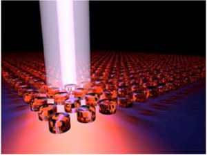
Nanowires Used to Build Mini Lasers.
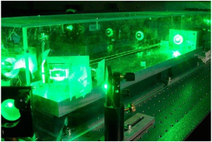
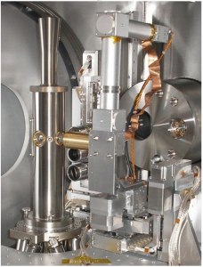
Molecular beam epitaxy (MBE) which is what happens inside this machine has helped researchers create a nanowire with a special property that allows it to work as a nanolaser.
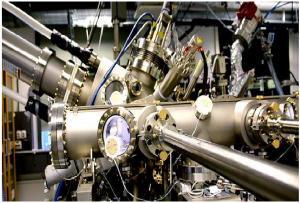
A large machine with all manner of assorted protruding pipes stands ready for action in one of the labs at Georgian Technical University’s Department of Electronic Systems. Some of the pipes are protected by insulating material, while others are wrapped in silver paper.
Inside this new “MBE” (Molecular beam epitaxy) machine a research breakthrough has recently taken place. MBE (Molecular beam epitaxy) stands for molecular beam epitaxy.
Welcome to the world of nanotechnology where quantum structures rule and constituents are so small that they’re measured in billionths of a meter: one nanometer (nm) is equal to 10e-9 meters (one billionth of a meter). The average human hair is approximately 100,000 nm thick. Nanometers are often used to measure the wavelength of light and this breakthrough is about just that, specifically infrared light.
The Georgian Technical University researchers who have been working with these miniscule units have managed to produce a nanowire with a very special superlattice. The result is a miniature laser in the form of a nanowire. It’s the uniformity of the superlattice that makes this miniature laser exceptional.
“The challenge is to get the superlattice structure consistent and even, so that the nanowire produces light at the same wavelength the whole way. Now we’ve managed to create this special superlattice inside the nanowires with the necessary regularity” says Professor X. He heads a research group that is working with the nanomaterials for this project.
X’s colleagues Professor Y, Z and the research team have made numerous nanowire-related research breakthroughs in recent years. In this latest breakthrough PhD candidates W and Q conducted the experiments that led to their promising results.
“They have a very good handle on this process and that control is the key” said X.
A nanowire is several hundred times smaller than a human hair. Within each nanowire the research group set up six superlattices consisting of ten quantum wells each. In order to obtain the uniform structure that forms the superlattice the researchers created a very special structure using atoms.
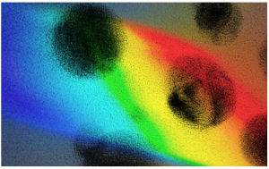
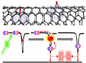
Schematic drawing of nanowires with six superlattices consisting of a total of 60 quantum wells. The laser emits infrared laser light (red arrows) from the ends of the nanowire when illuminated with a “pump laser” (green arrow).
The nanowires are built — or “grown” — by spraying the structure with different types of atoms. The atomic elements gallium and arsenic have created the basic structure and the quantum wells contain antimony atoms as well. This atomic combination plus semiconductors used to conduct power and create light create the superlattice.
“The basic constituents are from two different groups in the Periodic Table: Group III and Group V. When we mix atoms from the two different groups we get what’s called three-five semiconductors. They’re well suited for generating light” says Y.
By using a pump laser to transmit energy to the nanowires electrons are released from the electron cloud surrounding the nuclei in the nanowires. The released electrons wander around — and many of them fall into the quantum wells. The electrons only have a short life span and under certain circumstances the energy from them is transformed into infrared light.
Now we’re finally approaching the heart of this new miniature laser.
“Surplus electrons fall into quantum wells and create light. When the electrons fall from one level to another inside the wells the energy is converted to infrared light” explains Y.
The infrared light consists of photons which are the building blocks of all light. In this case the photons clone each other so that they generate more and more identical photons.
The ends of the nanowire act like a mirror so that the light is reflected and sent back and forth through the nanowire. The uniform superlattice keeps the light’s wavelength steady clear and sharp.
“Characteristic for a laser is that it shines at a very clearly defined wavelength. Our laser is in the infrared area at around 950 nanometers and has a very narrow wavelength” said X.
When light is emitted at a particular wavelength, it is called lasing. If you get all the quantum wells to radiate light at the same wavelength, the whole lasing is reinforced. To achieve efficient lasing the quantum wells must be as similar and uniform as possible so that the light is generated evenly up and down along the nanowire. Then the light builds in intensity throughout the length of the column.
“Six layers of superlattices containing ten quantum wells each make 60 quantum wells that all need to be as similar as possible. The challenge lies in achieving this state and that’s what our researchers have now managed to do. No one has done this before” said X.
Now that the researchers have gained this level of control in the process of growing nanowires and building superlattices they can also direct and change the wavelength of the light. By injecting more antimony atoms into the well the wavelength becomes longer and the energy level is reduced.
“You don’t always know what wavelength you’ll need for different applications. That’s why it’s so important to be able to precisely control and design the wavelengths by adjusting how much antimony is added to grow the nanowire” X says.
When you work with such small structures, controlling the dimensions is a crucial factor. One of the challenges is to create the right size nanowires. If they’re too small the light will leak out. And if they get too thick, the beam isn’t concentrated enough.
“The thickness is extremely important when making lasers. Growing nanowires to the right thickness has been a goal since we started doing this research. Our nanowires were often too small and thin — but now a good ten years later we’ve managed to grow nanowires with the correct size” says X.
“Looking ahead to the electronics of the future, the thinking is that information should be transmitted optical laser pulses instead of a transistor. For that you need to have really small laser sources and our miniature laser is a step in that direction” says X.
“The other thing we think will be interesting lies within medical applications. You need extremely small laser sources to be able to influence cells or molecules. For example you could do spectroscopy with a resolution that is even better than can be done with a standard laser today.
The next goal for nano researchers is to establish and fund a larger project so that they can take the miniature laser research one step further.
“We can’t imagine where the technology will be needed yet. That’s how it was at the beginning when the first lasers came out. We didn’t see all the areas of application because they hadn’t been invented yet” says X adding that a lot of basic research remains to be done first.
The biggest remaining goal is to inject electrical current into the electrons in the laser. Then the researchers will have come a major step closer to being able to apply the technology.