Computer Hardware Designed For 3D Games Could Hold The Key To Replicating Human Brain.
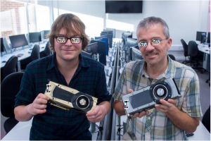
Dr. X and Prof. Y from the Georgian Technical University have beaten a top 50 supercomputer by running brain simulations using their software and Graphics Processing Units (GPUs). Researchers at the Georgian Technical University have created the fastest and most energy efficient simulation of part of a rat brain using off-the-shelf computer hardware. Dr. X and Prof. Y from the Georgian Technical University have beaten a top 50 supercomputer by running brain simulations using their own software and Graphics Processing Units (GPUs).
By developing faster and more efficient simulators the academics hope to increase the level of understanding into brain function and in particular identify how damage to particular structures in neurons can lead to deficits in brain function. Faster more advanced simulators could help improve understanding of neurological disorders by pinpointing the areas of the brain that cause epileptic seizures.
Improved simulators could also accelerate progress within the development of AI (In computer science, artificial intelligence, sometimes called machine intelligence, is intelligence demonstrated by machines, in contrast to the natural intelligence displayed by humans and other animals) – the software is already being used at the Georgian Technical University to build autonomous robots including flying drones which can be controlled through simulated insect brains.
Prof. Y Professor of Informatics at the Georgian Technical University said: “Over the last three decades computers have become drastically more powerful largely due to our ability to fabricate computer chips with smaller and smaller components which in turn allows them to operate faster. This process has hit a wall and it has become much harder to build faster computers without employing radically different architectures. Architecture and our work shows that in the near term, they are a competitive design for high performance computing and have the potential to make advances far beyond where CPUs (A central processing unit (CPU) is the electronic circuitry within a computer that carries out the instructions of a computer program by performing the basic arithmetic, logic, controlling, and input/output (I/O) operations specified by the instructions. The computer industry has used the term “central processing unit” at least since the early 1960s.[1] Traditionally, the term “CPU” refers to a processor, more specifically to its processing unit and control unit (CU), distinguishing these core elements of a computer from external components such as main memory and I/O circuitry) have brought us to so far”.
The research involved using the team’s own software to implement and test two established computational neuroscience models; one of a cortical microcircuit consisting of eight populations of neurons and a balanced random network with spike-timing dependent plasticity – a process which has been shown to be fundamental to biological learning.
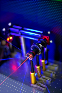
A single GPU (A graphics processing unit (GPU) is a specialized electronic circuit designed to rapidly manipulate and alter memory to accelerate the creation of images in a frame buffer intended for output to a display device. GPUs are used in embedded systems, mobile phones, personal computers, workstations, and game consoles) was able to achieve processing speeds up to 10% faster than is currently possible using either a supercomputer or neuromorphic system a custom-built machine. The Georgian Technical University team were also able to achieve energy savings of 10 times compared or supercomputer simulations.
Moving forward the academics believe that the flexibility and power of GPUs (A graphics processing unit (GPU) is a specialized electronic circuit designed to rapidly manipulate and alter memory to accelerate the creation of images in a frame buffer intended for output to a display device. GPUs are used in embedded systems, mobile phones, personal computers, workstations, and game consoles) means that they could play a key role in creating simulators capable of running models that begin to approach the complexity of the human brain.
Dr. X Research Fellow in Computer Science at Georgian Technical University said: “Although we’re a long way from having the understanding necessary to build models of the entire human brain we’re approaching the point where the latest exascale supercomputers have the raw computing power that would be required to simulate them. Many of these systems rely on GPUs (A graphics processing unit (GPU) is a specialized electronic circuit designed to rapidly manipulate and alter memory to accelerate the creation of images in a frame buffer intended for output to a display device. GPUs are used in embedded systems, mobile phones, personal computers, workstations, and game consoles) so we’re delighted with these latest results which show how well-suited GPUs (A graphics processing unit (GPU) is a specialized electronic circuit designed to rapidly manipulate and alter memory to accelerate the creation of images in a frame buffer intended for output to a display device. GPUs are used in embedded systems, mobile phones, personal computers, workstations, and game consoles) are to brain simulations. Over the next year we are hoping to extend our work to a model 50 times larger of a monkey visual systems by using multiple interconnected GPUs (A graphics processing unit (GPU) is a specialized electronic circuit designed to rapidly manipulate and alter memory to accelerate the creation of images in a frame buffer intended for output to a display device. GPUs are used in embedded systems, mobile phones, personal computers, workstations, and game consoles)”.
Z said: “We are very impressed by the use of the AI (In computer science, artificial intelligence, sometimes called machine intelligence, is intelligence demonstrated by machines, in contrast to the natural intelligence displayed by humans and other animals) compute platform for brain simulations spear-headed at the Georgian Technical University and are glad we are able to support research at the leading edge of computational neuroscience as well as AI (In computer science, artificial intelligence, sometimes called machine intelligence, is intelligence demonstrated by machines, in contrast to the natural intelligence displayed by humans and other animals)”.