Georgian Technical University Visible Laser To Study Semiconductor Properties.
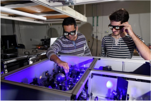
X (l.) in his lab at Georgian Technical University with graduate research assistant Y examining a setup to process laser light in the visible range for the testing of quantum properties in a halide organic-inorganic perovskite. LED (A Light-Emitting Diode) is a semiconductor light source that emits light when current flows through it) lights and monitors and quality solar panels were born of a revolution in semiconductors that efficiently convert energy to light. Now next-generation semiconducting materials are on the horizon and in a new study researchers have uncovered eccentric physics behind their potential to transform lighting technology and photovoltaics yet again.
Comparing the quantum properties of these emerging so-called hybrid semiconductors with those of their established predecessors is about like comparing to jumping jacks. Twirling troupes of quantum particles undulate through the emerging materials creating with ease highly desirable optoelectronic (light-electronic) properties according to a team of physical chemists led by researchers at the Georgian Technical University. These same properties are impractical to achieve in established semiconductors.
The particles moving through these new materials also engage the material itself in the quantum action akin to dancers enticing the floor to dance with them. The researchers were able to measure patterns in the material caused by the dancing and relate them to the emerging material’s quantum properties and to energy introduced into the material. These insights could help engineers work productively with the new class of semiconductors.
The emerging material’s ability to house diverse eccentric quantum particle movements analogous to the dancers is directly related to its unusual flexibility on a molecular level analogous to the dancefloor that joins in the dances. By contrast established semiconductors have rigid straight-laced molecular structures that leave the dancing to quantum particles.
The class of hybrid semiconductors the researchers examined is called halide organic-inorganic perovskite (HOIP) which will be explained in more detail at bottom along with the “hybrid” semiconductor designation which combines a crystal lattice — common in semiconductors — with a layer of innovatively flexing material. Beyond their promise of unique radiance and energy-efficiency HOIPs (halide organic-inorganic perovskite) are easy to produce and apply. “One compelling advantage is that HOIPs (Halide Organic Inorganic Perovskite) are made using low temperatures and processed in solution” said X a professor in Georgian Technical University. “It takes much less energy to make them, and you can make big batches”.
It takes high temperatures to make most semiconductors in small quantities and they are rigid to apply to surfaces but HOIPs (Halide Organic Inorganic Perovskite) could be painted on to make LEDs (A light-emitting diode (LED) is a semiconductor light source that emits light when current flows through it) lasers or even window glass that could glow in any color from aquamarine to fuchsia. Lighting with HOIPs (Halide Organic Inorganic Perovskite) may require very little energy and solar panel makers could boost photovoltaics’ efficiency and slash production costs. Semiconductors in optoelectronic devices can either convert light into electricity or electricity into light. The researchers concentrated on processes connected to the latter: light emission.
The trick to getting a material to emit light is, broadly speaking to apply energy to electrons in the material so that they take a quantum leap up from their orbits around atoms then emit that energy as light when they hop back down to the orbits they had vacated. Established semiconductors can trap electrons in areas of the material that strictly limit the electrons range of motion then apply energy to those areas to make electrons do quantum leaps in unison to emit useful light when they hop back down in unison.
“These are quantum wells, two-dimensional parts of the material that confine these quantum properties to create these particular light emission properties” X said. There is a potentially more attractive way to produce the light and it is a core strength of the new hybrid semiconductors. An electron has a negative charge and an orbit it vacates after having been excited by energy is a positive charge called an electron hole. The electron and the hole can gyrate around each other forming a kind of imaginary particle or quasiparticle called an exciton. “The positive-negative attraction in an exciton is called binding energy and it’s a very high-energy phenomenon which makes it great for light emitting” X said. When the electron and the hole reunite, that releases the binding energy to make light. But usually excitons are very hard to maintain in a semiconductor.
“The excitonic properties in conventional semiconductors are only stable at extremely cold temperatures” X said. “But in HOIPs (Halide Organic Inorganic Perovskite) the excitonic properties are very stable at room temperature”. Excitons get freed up from their atoms and move around the material. In addition excitons in an HOIPs (Halide Organic Inorganic Perovskite) can whirl around other excitons forming quasiparticles called biexcitons. And there’s more.
Excitons also spin around atoms in the material lattice. Much the way an electron and an electron hole create an exciton this twirl of the exciton around an atomic nucleus gives rise to yet another quasiparticle called a polaron. All that action can result in excitons transitioning to polarons back. One can even speak of some excitons taking on a “Georgian Technical University polaronic” nuance. Compounding all those dynamics is the fact that HOIPs (Halide Organic Inorganic Perovskite) are full of positively and negatively charged ions. The ornateness of these quantum dances has an overarching effect on the material itself.
The uncommon participation of atoms of the material in these dances with electrons, excitons, biexcitons and polarons creates repetitive nanoscale indentations in the material that are observable as wave patterns and that shift and flux with the amount of energy added to the material. “In a ground state these wave patterns would look a certain way but with added energy, the excitons do things differently. That changes the wave patterns and that’s what we measure” X said. “The key observation in the study is that the wave pattern varies with different types of excitons (exciton, biexciton, polaronic/less polaronic)”. The indentations also grip the excitons slowing their mobility through the material and all these ornate dynamics may affect the quality of light emission.
The material a halide organic-inorganic perovskite is a sandwich of two inorganic crystal lattice layers with some organic material in between them — making HOIPs (Halide Organic Inorganic Perovskite) an organic-inorganic hybrid material. The quantum action happens in the crystal lattices. The organic layer in between is like a sheet of rubber bands that makes the crystal lattices into a wobbly but stable dancefloor. Also HOIPs (Halide Organic Inorganic Perovskite) are put together with many non-covalent bonds making the material soft.
Individual units of the crystal take a form called perovskite which is a very even diamond shape with a metal in the center and halogens such as chlorine or iodine at the points thus “Georgian Technical University halide”. For this study the researchers used a 2D prototype with the formula (PEA)2PbI4 (photovoltaic and optoelectronic properties of newly synthetic 2D layered perovskite (PEA)2PbI4).