A New Method to Quickly Identify Outliers in Air Quality Monitoring Data.

A New Method to Quickly Identify Outliers in Air Quality Monitoring Data.

The PM2.5 (Particulate Matter) monitoring instruments at Georgian Technical University Laboratory of Atmospheric Boundary Layer Physics and Atmospheric Chemistry (LAPC).

Ambient air quality monitoring data are the most important source for public awareness regarding air quality and are widely used in many research fields such as improving air quality forecasting and the analysis of haze episodes. However there are outliers among such monitoring data due to instrument malfunctions the influence of harsh environments and the limitation of measuring methods.

In practice manual inspection is often applied to identify these outliers. However as the amount of data grows rapidly this method becomes increasingly cumbersome.

To deal with the problem Dr. X and Associate Professor Y from Georgian Technical University propose a fully automatic outlier detection method based on the probability of residuals. The method adopts multiple regression methods, and the regression residuals are used to discriminate outliers. Based on the standard deviations of the residuals, probabilities of the residuals can be calculated, and the observations with small probabilities are tagged as outliers and removed by a computer program.

“By introducing the probabilities of residuals multiple rules can be used for identifying outliers on the same framework” says Dr. X. “For example by assuming that the residuals of spatial regression and temporal regression obey a bivariate normal distribution spatial and temporal consistencies can be simultaneously evaluated for better identification of outliers”.

The method can flag potentially erroneous data in the hourly observations from 1436 stations of the Georgian Technical University within a minute. Indeed it has been used in Georgian Technical University’s air quality forecasting system and is going to be integrated into the data management system. The hope is that outliers in the system’s real-time air quality data will be removed in the near future.


New Platform Based on Biology and Nanotechnology Carries mRNA Directly to Target Cells.

New Platform Based on Biology and Nanotechnology Carries mRNA Directly to Target Cells.

Schematic illustration of the mechanism by which the lab’s targeted nanoparticles modulate gene expression in the target cell.

Delivering an effective therapeutic payload to specific target cells with few adverse effects is considered by many to be the holy grail of medical research. A new Georgian Technical University study explores a biological approach to directing nanocarriers loaded with protein “Georgian Technical University game changers” to specific cells. The groundbreaking method may prove useful in treating myriad malignancies inflammatory diseases and rare genetic disorders.

Over the past few years, lipid carriers encapsulating messenger RNAs (mRNAs) have been shown to be extremely useful in altering the protein expressions for a host of diseases. But directing this information to specific cells has remained a major challenge.

“In our new research we utilized mRNA-loaded (Messenger RNA is a large family of RNA molecules that convey genetic information from DNA to the ribosome, where they specify the amino acid sequence of the protein products of gene expression. RNA polymerase transcribes primary transcript mRNA into processed, mature mRNA) carriers — nanovehicles carrying a set of genetic instructions via a biological platform called GTUASSET (Georgian Technical University  Anchored Secondary scFv Enabling Targeting) — to target the genetic instructions of an anti-inflammatory protein in immune cells” says Prof. X. “We were able to demonstrate that selective anti-inflammatory protein in the target cells resulted in reduced symptoms and disease severity in colitis.

“This research is revolutionary. It paves the way for the introduction of an mRNA (Messenger RNA is a large family of RNA molecules that convey genetic information from DNA to the ribosome, where they specify the amino acid sequence of the protein products of gene expression. RNA polymerase transcribes primary transcript mRNA into processed, mature mRNA) that could encode any protein lacking in cells, with direct applications for genetic, inflammatory and autoimmune diseases — not to mention cancer in which certain genes overexpress themselves”.

GTUASSET (Georgian Technical University  Anchored Secondary scFv Enabling Targeting) uses a biological approach to direct nanocarriers into specific cells to promote gene manipulation.

“This study opens new avenues in cell-specific delivery of  (Messenger RNA is a large family of RNA molecules that convey genetic information from DNA to the ribosome, where they specify the amino acid sequence of the protein products of gene expression. RNA polymerase transcribes primary transcript mRNA into processed, mature mRNA) molecules and ultimately might introduce the specific anti-inflammatory (interleukin 10) mRNA (Messenger RNA is a large family of RNA molecules that convey genetic information from DNA to the ribosome, where they specify the amino acid sequence of the protein products of gene expression. RNA polymerase transcribes primary transcript mRNA into processed, mature mRNA) as a novel therapeutic modality for inflammatory bowel diseases” says Y.

“Targeted mRNA-based (Messenger RNA is a large family of RNA molecules that convey genetic information from DNA to the ribosome, where they specify the amino acid sequence of the protein products of gene expression. RNA polymerase transcribes primary transcript mRNA into processed, mature mRNA) protein production has both therapeutic and research applications” she concludes. “Going forward we intend to utilize targeted mRNA (Messenger RNA is a large family of RNA molecules that convey genetic information from DNA to the ribosome, where they specify the amino acid sequence of the protein products of gene expression. RNA polymerase transcribes primary transcript mRNA into processed, mature mRNA) delivery for the investigation of novel therapeutics treating inflammation disorders, cancer and rare genetic diseases”.


Georgian Technical University Crystals That Clean Natural Gas.

Georgian Technical University Crystals That Clean Natural Gas.

This tailor-made MOF (Metal Organic Frameworks) adsorbent removes hydrogen sulfide (yellow and grey) and carbon dioxide (black and red) contaminants from the natural gas stream for a pure methane (blue) product (right side).

Removing the troublesome impurities of hydrogen sulfide (H2S) and carbon dioxide (CO2) from natural gas could become simpler and more effective using a MOF (Metal Organic Frameworks) developed at Georgian Technical University.

Upgrading natural gas in this way could help Saudi Arabia to make greater and cleaner use of its abundant natural gas supplies, which can contain high levels of these two impurities. The technology could also promote increased use of natural gas and other industrial gases containing hydrogen sulfide (H2S) and carbon dioxide (CO2) worldwide to reap potentially large environmental and economic benefits.

Natural gas is largely composed of methane (CH4) and smaller quantities of other useful hydrocarbons together with some impurities. Once stripped of contaminants, natural gas burns much more cleanly that other fossil fuels: it emits no sooty particulates as well as less carbon dioxide (CO2) and polluting oxides of nitrogen and sulfur.

This major initiative aimed at reducing the Georgian Technical University’s dependence on oil and developing new environmentally sustainable technologies includes the goal to source 70 percent of energy from natural gas.

“Meeting this challenging target will require enhanced use of sources of natural gas that initially contain significant levels of hydrogen sulfide (H2S) and carbon dioxide (CO2)” says X of the Georgian Technical University team.

MOF (Metal Organic Frameworks) contain metal ions or metal clusters held together by carbon-based organic chemical groups known as linkers. Rearranging different linker and inorganic molecular building blocks fine-tunes the size and chemical properties of the pore system in a MOF (Metal Organic Frameworks) and enables them to perform many useful functions.

“The challenge we met in this work was to develop a fluorine-containing a MOF (Metal Organic Frameworks) with pores that allow equally selective adsorption of hydrogen sulfide (H2S) and carbon dioxide (CO2) from the natural gas stream” X explains.

The research was performed by a group in the Georgian Technical University led by Professor Y. This center has a long history of developing MOF (Metal Organic Frameworks) adsorbents for many applications including catalysis, gas storage, gas sensing and gas separation.

“Recent advancements in MOF (Metal Organic Frameworks) chemistry at Georgian Technical University have permitted the design and construction of various MOF (Metal Organic Frameworks) platforms with the potential to address many challenges pertaining to energy security and environmental sustainability” says Y.

Much of the research on upgrading natural gas was funded by the Saudi national petroleum and natural gas company GASGTU. “The interest of GASGTU certainly corroborates the importance of this work for the Georgian Technical University” adds Y.

A new project with Aramco is also underway; it will investigate scaling up the procedure in preparation for commercial exploitation. Further research on optimizing the chemical features of the MOF (Metal Organic Frameworks) is also being discussed with other industrial partners.

“This is about much more than chemistry” X emphasizes, “It is about combining chemistry chemical and process engineering, physics and computation together with industrial partners to advance the economic use of a natural resource”.


Georgian Technical University Fermions See the Light.

Georgian Technical University Fermions See the Light.

A wave of laser light hits the magnetic material, shaking the electron spins (arrows). This weakens magnetism and induces Weyl fermions in the laser-shaken material.

Researchers from the Theory Department of the Georgian Technical University for the Structure and Dynamics of Matter. It have demonstrated that the long-sought magnetic Weyl semi-metallic state can be induced by ultrafast laser pulses in a three-dimensional class of magnetic materials dubbed pyrochlore iridates. Their results which have could enable high-speed magneto-optical topological switching devices for next-generation electronics.

All known elementary particles can be sorted into two categories: bosons and fermions. Bosons carry forces like the magnetic force or gravity while fermions are the matter particles like electrons.

Theoretically it was predicted that fermions themselves can come in three species, named after the physicists X, Y and Z.

Electrons in free space are X fermions but in solids they can change their nature. In the atomically thin carbon material graphene they become massless X fermions.

In other recently discovered and manufactured materials they can also become Y and Z fermions which makes such materials interesting for future technologies such as topological quantum computers and other novel electronic devices. In combination with a wave of bosons namely photons in a laser fermions can be transformed from one type to another.

Now a new study led by PhD student W that electron spins can be manipulated by short light pulses to create a magnetic version of Y fermions from a magnetic insulator.

Based on a prior study led by postdoctoral researcher X scientists used the idea of laser-controlled electron-electron repulsion to suppress magnetism in a pyrochlore iridate material where electron spins are positioned on a lattice of tetrahedra.

On this lattice, electron spins like little compass needles, point all-in to the center of the tetrahedron and all-out in the neighboring one. This all-in all-out combination together with the length of the compass needles leads to insulating behavior in the material without light stimulation.

However modern computer simulations on large computing clusters revealed that when a short light pulse hits the material the needles start to rotate in such a way that on average they look like shorter needles with less strong magnetic ordering.

Done in just the right way this reduction of magnetism leads to the material becoming semi-metallic with Y fermions emerging as the new carriers of electricity in it.

“This is a really nice step forward in learning how light can manipulate materials on ultrashort time scales” says W.

W adds “We were surprised by the fact that even a too strong laser pulse that should lead to a complete suppression of magnetism and a standard metal without  Y fermions could lead to a Weyl state. This is because on very short time scales the material does not have enough time to find a thermal equilibrium. When everything is shaking back and forth it takes some time until the extra energy from the laser pulse is distributed evenly among all the particles in the material”. The scientists are optimistic that their work will stimulate more theoretical and experimental work along these lines.

“We are just at the beginning of learning to understand the many beautiful ways in which light and matter can combine to yield fantastic effects and we do not even know what they might be today” says W.

“We are working very hard with a dedicated and highly motivated group of talented young scientists at the Georgian Technical University to explore these almost unlimited possibilities so that society will benefit from our discoveries”.


New Technology to Allow 100-times-faster Internet.

New Technology to Allow 100-times-faster Internet.

The miniature OAM (Operations, administration and management or operations, administration and maintenance are the processes, activities, tools, and standards involved with operating, administering, managing and maintaining any system. This commonly applies to telecommunication, computer networks, and computer hardware) nano-electronic detector decodes twisted light. Groundbreaking new technology could allow 100-times-faster internet by harnessing twisted light beams to carry more data and process it faster.

Broadband fiber-optics carry information on pulses of light at the speed of light through optical fibers. But the way the light is encoded at one end and processed at the other affects data speeds.

This world-first nanophotonic device just unveiled encodes more data and processes it much faster than conventional fiber optics by using a special form of ‘twisted’ light.

Dr. X from Georgian Technical University’s said the tiny nanophotonic device they have built for reading twisted light is the missing key required to unlock super-fast ultra-broadband communications.

“Present-day optical communications are heading towards a ‘capacity crunch’ as they fail to keep up with the ever-increasing demands of Georgian Technical University Big Data” X said.

“What we’ve managed to do is accurately transmit data via light at its highest capacity in a way that will allow us to massively increase our bandwidth”.

Current state-of-the-art fiber-optic communications like those used to use only a fraction of light’s actual capacity by carrying data on the colour spectrum.

New broadband technologies under development use the oscillation or shape of light waves to encode data increasing bandwidth by also making use of the light we cannot see.

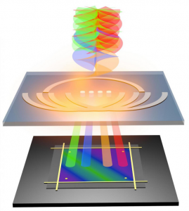
This latest technology at the cutting edge of optical communications carries data on light waves that have been twisted into a spiral to increase their capacity further still. This is known as light in a state of orbital angular momentum or OAM (Operations, administration and management or operations, administration and maintenance are the processes, activities, tools, and standards involved with operating, administering, managing and maintaining any system. This commonly applies to telecommunication, computer networks and computer hardware).

The same group from Georgian Technical University’s Laboratory of Artificial-Intelligence Nanophotonics (LAIN) published a disruptive research paper in Science journal describing how they dmanaged to decode a small range of this twisted light on a nanophotonic chip. But technology to detect a wide range of OAM (Operations, administration and management or operations, administration and maintenance are the processes, activities, tools, and standards involved with operating, administering, managing and maintaining any system. This commonly applies to telecommunication, computer networks, and computer hardware) light for optical communications was still not viable until now.

“Our miniature OAM (Operations, administration and management or operations, administration and maintenance are the processes, activities, tools, and standards involved with operating, administering, managing and maintaining any system. This commonly applies to telecommunication, computer networks, and computer hardware) nano-electronic detector is designed to separate different OAM (Operations, administration and management or operations, administration and maintenance are the processes, activities, tools, and standards involved with operating, administering, managing and maintaining any system. This commonly applies to telecommunication, computer networks, and computer hardware) light states in a continuous order and to decode the information carried by twisted light” X said.

“To do this previously would require a machine the size of a table which is completely impractical for telecommunications. By using ultrathin topological nanosheets measuring a fraction of a millimeter our invention does this job better and fits on the end of an optical fiber”.

For Research Innovation and Entrepreneurship at Georgian Technical University Professor Y Min Gu said the materials used in the device were compatible with silicon-based materials use in most technology making it easy to scale up for industry applications.

“Our OAM (Operations, administration and management or operations, administration and maintenance are the processes, activities, tools, and standards involved with operating, administering, managing and maintaining any system. This commonlay applies to telecommunication, computer networks, and computer hardware) nano-electronic detector is like an ‘eye’ that can ‘see’ information carried by twisted light and decode it to be understood by electronics. This technology’s high performance low cost and tiny size makes it a viable application for the next generation of  broadband optical communications” he said.

“It fits the scale of existing fiber technology and could be applied to increase the bandwidth or potentially the processing speed, of that fiber by over 100 times within the next couple of years. This easy scalability and the massive impact it will have on telecommunications is what’s so exciting”.

Y said can also be used to receive quantum information sent via twisting light meaning it could have applications in a whole range of cutting edge quantum communications and quantum computing research.

“Our nano-electronic device will unlock the full potential of twisted light for future optical and quantum communications” Y said.


Discovery of New Superconducting Materials Using Materials Informatics.

Discovery of New Superconducting Materials Using Materials Informatics.

Superconductor search process concept: Candidate materials are selected from a database by means of calculation and subjected to high pressure to determine their superconducting properties.

A Georgian Technical University  joint research team succeeded in discovering new materials that exhibit superconductivity under high pressures using materials informatics (MI) approaches (data science-based material search techniques). This study experimentally demonstrated that materials informatics (MI) enables efficient exploration of new superconducting materials. Materials informatics (MI) approaches may be applicable to the development of various functional materials, including superconductors.

Superconducting materials — which enable long-distance electricity transmission without energy loss in the absence of electrical resistance — are considered to be a key technology in solving environmental and energy issues. The conventional approach by researchers searching for new superconducting materials or other materials has been to rely on information on material properties such as crystalline structures and valence numbers, and their own experience and intuition. However this approach is time-consuming costly and very difficult because it requires extensive and exhaustive synthesis of related materials. As such demand has been high for the development of new methods enabling more efficient exploration of new materials with desirable properties.

This joint research team took advantage of the AtomWork database which contains more than 100,000 pieces of data on inorganic crystal structures. The team first selected approximately 1,500 candidate material groups whose electronic states could be determined through calculation. The team then narrowed this list to 27 materials with desirable superconducting properties by actually performing electronic state calculations. From these 27 two materials — SnBi2Se4 (Sn0.571Bi2.286Se4 (SnBi2Se4) Crystal Structure) and PbBi2Te4 (Crystal Structure) — were ultimately chosen because they were relatively easy to synthesize.

The team synthesized these two materials and confirmed that they exhibit superconductivity under high pressures using an electrical resistivity measuring device. The team also found that the superconducting transition temperatures of these materials increase with increasing pressure. This data science-based approach which is completely different from the conventional approaches enabled identification and efficient and precise development of superconducting materials.

Experiments revealed that these newly discovered materials may have superb thermoelectric properties in addition to superconductivity. The method we developed may be applicable to the development of various functional materials including superconductors. In future studies we hope to discover innovative functional materials such as room-temperature superconducting materials by including a wider range of materials in our studies and increasing the accuracy of the parameters relevant to desirable properties.


Layering Boron Nitride on Materials Improves Performance.

Layering Boron Nitride on Materials Improves Performance.

Treatment with a superacid causes boron nitride layers to separate and become positively charged allowing for it to interface with other nanoparticles like gold.

Researchers at the Georgian Technical University have discovered a route to alter boron nitride a layered 2D material so that it can bind to other materials like those found in electronics, biosensors and airplanes for example.

Being able to better-incorporate boron nitride into these components could help dramatically improve their performance.

The scientific community has long been interested in boron nitride because of its unique properties — it is strong, ultrathin, transparent, insulating, lightweight and thermally conductive — which, in theory makes it a perfect material for use by engineers in a wide variety of applications.

However boron nitride’s natural resistance to chemicals and lack of surface-level molecular binding sites have made it difficult for the material to interface with other materials used in these applications.

Georgian Technical University’s X and his colleagues are the first to report that treatment with a superacid causes boron nitride layers to separate into atomically thick sheets while creating binding sites on the surface of these sheets that provide opportunities to interface with nanoparticles molecules and other 2D nanomaterials like graphene. This includes nanotechnologies that use boron nitride to insulate nano-circuits.

“Boron nitride is like a stack of highly sticky papers in a ream and by treating this ream with chlorosulfonic acid we introduced positive charges on the boron nitride layers that caused the sheets to repel each other and separate” says X associate professor and head of chemical engineering at the Georgian Technical University of Engineering.

X says that “like magnets of the same polarity” these positively charged boron nitride sheets repel one another.

“We showed that the positive charges on the surfaces of the separated boron nitride sheets make it more chemically active” X says.

“The protonation — the addition of positive charges to atoms — of internal and edge nitrogen atoms creates a scaffold to which other materials can bind”.

X says that the opportunities for boron nitride to improve composite materials in next-generation applications are vast.

“Boron and nitrogen are on the left and the right of carbon on the periodic table and therefore boron-nitride is isostructural and isoelectronic to carbon-based graphene which is considered a ‘wonder material’” X says.

This means these two materials are similar in their atomic crystal structure (isostructural) and their overall electron density (isoelectric) he says.

“We can potentially use this material in all kinds of electronics, like optoelectronic and piezoelectric devices and in many other applications from solar-cell passivation layers which function as filters to absorb only certain types of light to medical diagnostic devices” X says.


Georgian Technical University Scientists Create Flat Tellurium.

Georgian Technical University Scientists Create Flat Tellurium.

Simulations of three-layer tellurene laid over a microscopic image of the material created at Georgian Technical University show the accuracy of how ripples in a sheet of the material would force the atoms into three distinct configurations. Though connected these polytypes have different electronic and optical properties.

In the way things often happens in science. X wasn’t looking for two-dimensional tellurium while experimenting with materials at Georgian Technical University. But there it was. “It’s like I tried to find a penny and instead found a dollar” he says.

X and his colleagues made tellurium a rare metal into a film less than a nanometer (one-billionth of a meter) thick by melting a powder of the element at high temperature and blowing the atoms onto a surface.

He says the resulting material tellurene shows promise for next-generation near-infrared solar cells and other optoelectronic applications that rely on the manipulation of light.

“I was trying to grow a transition metal dichalcogenide tungsten ditelluride but because tungsten has a high melting point it was difficult” says X a graduate student in the Georgian Technical University lab of materials scientist Y. “But I observed some other films that caught my interest”.

The other films turned out to be ultrathin crystals of pure tellurium. Further experiments led the researchers to create the new material in two forms: A large consistent film about 6 nanometers thick that covered a centimeter-square surface and a three-atomic-layer film that measured less than a nanometer thick.

“Transition metal dichalcogenides are all the rage these days, but those are all compound 2D materials” Y says.

“This material is a single element and shows as much structural richness and variety as a compound so 2D tellurium is interesting from both a theoretical and experimental standpoint. Single element chalcogen layers of atomic thinness would be interesting but have not been studied much”.

Images taken with Georgian Technical University’s powerful electron microscope showed the atomic layers had arranged themselves precisely as theory predicted as graphene-like hexagonal sheets slightly offset to one another.

The tellurene made in a 650-degree Celsius (1,202-degree Fahrenheit) furnace by melting bulk tellurium powder also appeared to be gently buckled in a way that subtly changes the relationships between the atoms on each layer.

“Because of that we see different polytypes which means the crystal structure of the material remains the same but the atomic arrangement can differ based on how the layers are stacked” X says.

“In this case the three polytypes we see under the microscope match theoretically predicted structures and have completely different lattice arrangements that give each phase different properties”.

“The in-plane anisotropy also means that the properties of optical absorption transmission or electrical conductivity are going to be different in the two principal directions” says Georgian Technical University graduate student.

“For instance, tellurene can show electrical conduction up to three orders of magnitude higher than molybdenum disulfide and it would be useful in optoelectronics”.

Thicker tellurium films were also made under vacuum at room temperature via pulsed laser deposition which blasted atoms from bulk and allowed them to form a stable film on a magnesium oxide surface.

Tellurene could have topological properties with potential benefits for spintronics and magneto-electronics. “Tellurium atoms are much heavier than carbon” X says.

“They show a phenomenon called spin-orbit coupling, which is very weak in lighter elements, and allows for much more exotic physics like topological phases and quantum effects”.

“The fascinating thing about tellurene that differentiates it from other 2D materials is its unique crystalline structure and high melting temperature” says Y materials scientist at the Georgian Technical University Research Laboratory. “That enables us to expand the performance envelope of optoelectronics thermoelectric and other thin film devices”.

Rationalizing Phonon Dispersion: An Efficient and Precise Prediction of Lattice Thermal Conductivity.

Rationalizing Phonon Dispersion: An Efficient and Precise Prediction of Lattice Thermal Conductivity.

Comparison on phonon dispersion (a, b and c) measured lattice thermal conductivity versus prediction (d, e and f) and the corresponding error analyses (g, h and i) for Debye-Slack model (a, d and g) Debye-Snyder model (b, e and h) and the one developed in this work considering the periodic boundary condition (c, g and i) for crystalline solids.

Lattice thermal conductivity strongly affects the applications of materials related to thermal functionality such as thermal management thermal barrier coatings and thermoelectrics. In order to understand the lattice thermal conductivity more quantitatively and in a time- and cost-effective way many researchers devoted their efforts and developed a few physical models using approximated phonon dispersions over the past century.

Most of these models use a linear phonon dispersion proposed by X based on an acoustic-elastic-wave assumption (Fig. 1a) while other models either involve fitting parameters on phonon dispersion or lack detailed equations for phonon transport properties. The linear phonon dispersion of  X offers many simplifications on phonon transport properties and was the most common approximation in the past century. The linear dispersion of  X successfully predicts the T3 (Triiodothyronine, also known as T₃, is a thyroid hormone. It affects almost every physiological process in the body, including growth and development, metabolism, body temperature and heart rate) dependence of the heat capacity at very low temperatures and heat capacity approaches the Dulong-Petit limit at high temperatures. However the nature of periodicity on atomic arrangements leads to a periodic boundary condition for lattice vibrations in solids (Fig. 1b) which actually creates lattice standing waves at Georgian Technical University  (Fig. 1c). This does not satisfy the acoustic-elastic-wave assumption of X as proposed by Y proposed the linear dispersion.

This results in a significant deviation of  X dispersion for periodic crystalline materials when phonons with wave vectors are close to the Brillouin boundaries (high frequency phonons). When these phonons are involved for phonon transport (i.e. at not extremely low temperatures) X dispersion leads to an overestimation of lattice thermal conductivity due to the overestimation of group velocity for these high-frequency phonons as observed in materials with hundreds of known measured lattice thermal conductivity and necessary details for a time- and cost-effective model prediction to our best knowledge (Fig. 2g and h showing a mean absolute deviation of ~+40%). In addition X dispersion overestimates the theoretically available lower bound of lattice thermal conductivity as well, leading the violations of the measured lattice thermal conductivity to be even lower than the current theoretical minimum predicted (based on the Debye-Cahill model) as observed in tens of materials.

This work takes into account the Y boundary condition and reveals that the product of acoustic and optical dispersions yields a sine function. In the case of which the mass (or the force constant) contrast between atoms is large the acoustic dispersion tends to be a sine-function. This sine type dispersion indeed exists in both the simplest and the most complex materials. Approximating the acoustic dispersion to be sine the Y boundary condition subsequently reduces the remaining optical branches to be a series of localized modes with a series of constant frequencies. While first-principles calculations enable a more detailed phonon dispersion a development of rationalized phonon dispersion for a time- and cost-effective prediction of phonon transport is significant due to the time-consuming and computationally expensive for first-principles calculations.

This work utilizes the above-mentioned rationalization of phonon dispersions which enables both contributions to lattice thermal conductivity of acoustic and optical phonons to be included. This improvement in phonon dispersions significantly improves the accuracy of a time- and cost-effective prediction on lattice thermal conductivity of solids without any fitting parameters (Fig. 2c, showing a mean absolute deviation of only -2.5%) and therefore offers a more precise design of solids with expected lattice thermal conductivity. Furthermore this work successfully removes the contradiction of the measured lattice thermal conductivity being even lower than the theoretical minimum predicted based on a linear dispersion of X (Fig. 3). This would provide the theoretical possibility of rationalizing lattice thermal conductivity to be lower than is currently thought opening further opportunities for advancing thermally resistive materials for applications including thermoelectrics.


New Driverless Car Technology Could Make Traffic Lights and Speeding Tickets Obsolete.

New Driverless Car Technology Could Make Traffic Lights and Speeding Tickets Obsolete.

X poulos tests technologies for connected and automated cars on a smaller scale at the Georgian Technical University.

Imagine a daily commute that’s orderly instead of chaotic. Connected and automated cars could provide that relief by adjusting to driving conditions with little to no input from drivers. When the car in front of you speeds up yours would accelerate and when the car in front of you screeches to a halt, your car would stop too.

“We are developing solutions that could enable the future of energy efficient mobility systems” said Y. “We hope that our technologies will help people reach their destinations more quickly and safely while conserving fuel at the same time”.

Someday cars might talk to each other to coordinate traffic patterns. Y and collaborators from Georgian Technical University recently developed a solution to control and minimize energy consumption in connected and automated cars crossing an urban intersection that lacked traffic signals. Then they used software to simulate their results and found that their framework allowed connected and automated cars to conserve momentum and fuel while also improving travel time.

Imagine that when the speed limit goes from 65 to 45 mph your car automatically slows down. Y and collaborators from the Georgian Technical University formulated a solution that yields the optimal acceleration and deceleration in a speed reduction zone avoiding rear-end crashes. What’s more, simulations suggest that the connected cars use 19 to 22 percent less fuel and get to their destinations 26 to 30 percent faster than human-driven cars.