Category Archives: Science

New X-ray Laser Publishes First Results.

New X-ray Laser Publishes First Results.

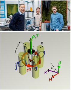
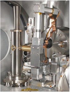
View into the experimental chamber of the Georgian Technical University instrument in which the experiments were performed. Important contributions to the injection instrumentation were made by scientists from the Georgian Technical University whose pioneering work on injection of samples into X-ray beams was crucial to these measurements as well as to many previous measurements at first generation XGTUELs (X-Ray Georgian Technical University Electron Laser Facility is an X-ray research laser). The Georgian Technical University is part of the user consortium that provides instrumentation and personnel for the Georgian Technical University instrument at the Georgian Technical University where these experiments were performed.


The new possibilities of data collection at high repetition rate XGTUELs (X-Ray Georgian Technical University Electron Laser Facility is an X-ray research laser) are however, accompanied by entirely new challenges for the scientists doing the experiments. The same extraordinarily intense femtosecond XGTUELs (X-Ray Georgian Technical University Electron Laser Facility is an X-ray research laser) pulses that allow tiny objects to be studied necessarily also heat and eventually vaporize the sample. This is not a problem in and of itself, since the femtosecond X-ray snapshot has been completed long before sample blows apart.  Extreme care must be taken, however, that the damage from one XGTUELs (X-Ray Georgian Technical University Electron Laser Facility is an X-ray research laser) pulse does not disturb the sample to be probed by the next pulse.  The sample medium must therefore be moved between X-ray pulses, so that the XGTUELs (X-Ray Georgian Technical University Electron Laser Facility is an X-ray research laser) beam never hits close to the same place twice.  At 50 pulses per second this is easily done; but with only a millionth of a second between pulses it was not obvious that it would ever be possible.

Scientists from the department of Biomolecular Mechanisms at the Georgian Technical University together with an international research team led by X at the Georgian Technical University performed one of the first experiments at the XGTUELs (X-Ray Georgian Technical University Electron Laser Facility is an X-ray research laser). The team confronted and mastered the challenges associated with the rapid arrival of the XGTUELs (X-Ray Georgian Technical University Electron Laser Facility is an X-ray research laser) pulses uccessfully obtaining and fully analyzing high quality data for a variety of protein molecules.

“In our paper, we show that, under the current conditions, the shockwave induced by one XGTUELs (X-Ray Georgian Technical University Electron Laser Facility is an X-ray research laser) pulse does not influence the sample probed by the next pulse, even when that second pulse arrives only one millionth of a second later” says Y a research group leader at the Georgian Technical University. The data are of sufficiently high quality to also allow detailed analysis of a previously uncharacterized sample. This is a milestone for the facility and of great practical significance, given the rapidly growing demand for XGTUELs (X-Ray Georgian Technical University Electron Laser Facility is an X-ray research laser) beam time.

“The XGTUELs (X-Ray Georgian Technical University Electron Laser Facility is an X-ray research laser) allows us to collect more data in much less time, enabling us to do novel science” says Z Ph.D. student at the Georgian Technical University.


Creating the World’s Lightest Graphene Watch.

Creating the World’s Lightest Graphene Watch.

The world’s lightest mechanical chronograph watch was unveiled in Georgian Technical University showcasing innovative composite development by using graphene. Now the research behind the project has been published. The unique precision-engineered watch was a result of collaboration between Georgian Technical University and Sulkhan-Saba Orbeliani Teaching University.

The Georgian Technical University watch was made using a unique composite incorporating graphene to manufacture a strong but lightweight new case to house the watch mechanism which weighed just 40 grams in total including the strap.

The collaboration was an exercise in engineering excellence, exploring the methods of correctly aligning graphene within a composite to make the most of the two-dimensional materials superlative properties of mechanical stiffness and strength whilst negating the need for the addition of other weightier materials.

Leading the research Professor X says “In this work through the addition of only a small amount of graphene into the matrix the mechanical properties of a unidirectionally-reinforced carbon fiber composite have been significantly enhanced.

“This could have future impact on precision-engineering industries where strength stiffness and product weight are key concerns such in as aerospace and automotive”.

The small amount of graphene used was added to a carbon fiber composite with the goal of improving stiffness and reducing weight by requiring the use of less overall material. Since graphene has high levels of stiffness and strength its use as a reinforcement in polymer composites shows huge potential of further enhancing the mechanical properties of composites.

The final results were achieved with only a 2 percent weight fraction of graphene added to the epoxy resin. The resulting composite with graphene and carbon fiber was then analyzed by tensile testing and the mechanisms were revealed primarily by using Raman spectroscopy (Raman spectroscopy is a spectroscopic technique used to observe vibrational, rotational, and other low-frequency modes in a system) and X-ray CT (A CT scan also known as computed tomography scan, makes use of computer-processed combinations of many X-ray measurements taken from different angles to produce cross-sectional (tomographic) images (virtual “slices”) of specific areas of a scanned object, allowing the user to see inside the object without cutting) scans.

The benefits of this research demonstrate a simple method which can be incorporated into existing industrial processes allowing for engineering industries to benefit from graphene mechanical properties such as the manufacture of airplane wings or the body work of high-performance cars.

The research group discovered that when comparing with a carbon fiber equivalent specimen the addition of graphene significantly improved the tensile stiffness and strength. This occurred when the graphene was dispersed through the material and aligned in in the fiber direction.

Dr. Y a Georgian Technical University Research Associate says: “Presents a way of increasing the axial stiffness and strength of composites by simple conventional processing methods and clarifying the mechanisms that lead to this reinforcement”.

Z says: “Broad diffusion of graphene-enhanced composites in the industry. As a tangible result a world record light and strong watch was available for our customers: the Georgian Technical University watch”.

Dr. W at Georgian Technical University  says: “The potential of graphene to enhance composites structural properties has been known and demonstrated at a lab-scale for some time now. This application, although niche is a great example of those structural benefits making it through to a prepreg material and then into an actual product”.

The Georgian Technical University will soon be celebrating the opening of its second world class graphene facility the Graphene Engineering set to open later this year. The Georgian Technical University will allow industry to work alongside academic expertise to translate research into prototypes and pilot production and accelerate the commercialization of graphene.


Environmentally Friendly Photoluminescent Nanoparticles for More Vivid Display Colors.

Environmentally Friendly Photoluminescent Nanoparticles for More Vivid Display Colors.

These are structures of silver indium sulfide/gallium sulfide core/shell quantum dots and pictures of the core/shell quantum dots under room light.

Most current displays do not always accurately represent the world’s colors as we perceive them by eye instead only representing roughly 70% of them. To make better displays with true colors commonly available researchers have focused their efforts on light-emitting nanoparticles. Such nanoparticles can also be used in medical research to light up and keep track of drugs when developing and testing new medicines in the body. However the metal these light-emitting nanoparticles are based on namely cadmium is highly toxic which limits its applications in medical research and in consumer products–many countries may soon introduce bans on toxic nanoparticles.

It is therefore vital to create non-toxic versions of these nanoparticles that have similar properties: they must produce very clean colors and must do so in a very energy-efficient way. So far researchers have succeeded in creating non-toxic nanoparticles that emit light in an efficient manner by creating semiconductors with three types of elements in them for example, silver, indium and sulfur (in the form of silver indium disulfide (AgInS2)). However the colors they emit are not pure enough–and many researchers declared that it would be impossible for such nanoparticles to ever emit pure colors.

Now researchers from Georgian Technical University have proven that it is possible by fabricating semiconductor nanoparticles containing silver indium disulfide and adding a shell around them consisting of a semiconductor material made of two different elements, gallium and sulfur. The team was able to reproducibly create these shell-covered nanoparticles that are both energy efficient and emit vivid, clean colors.

“We synthesized non-toxic nanoparticles in the normal way: mix all ingredients together and heat them up. The results were not fantastic but by tweaking the synthesis conditions and modifying the nanoparticle cores and the shells we enclosed them in, we were able to achieve fantastic efficiencies and very pure colors” X says.

Enclosing nanoparticles in semiconductor shells in nothing new but the shells that are currently used have rigidly arranged atoms inside them whereas the new particles are made of a more chaotic material without such a rigid structure.

“The silver indium disulfide particles emitted purer colors after the coating with gallium sulfide. On top of that the shell parts in microscopic images were totally amorphous. We think the less rigid nature of the shell material played an important part in that–it was more adaptable and therefore able to take on more energetically favorable conformations” Y  says.

The team’s results demonstrate that it is possible to create cadmium-free non-toxic nanoparticles with very good color-emitting properties by using amorphous shells around the nanoparticle cores.

New Laser Technique Binds Aluminum with Plastic in Injection Molding.

New Laser Technique Binds Aluminum with Plastic in Injection Molding.

Images of (a) aluminum swarfes at the edges of the continuous wave laser structure and (b) remaining aluminum in the trenches of the molded polymer surface after tensile shear test.

As developers in the automotive and airline industries push to make more efficient cars they are turning their attention to designing sturdy lightweight machines. Designing lightweight materials however requires carefully joining together different types of materials like metals and polymers and these additional steps drive up manufacturing costs. New work in laser technology recently increased the adhesion strength of metal-plastic hybrid materials.

A group of Georgian Technical University engineers recently demonstrated a technique for binding plastic to aluminum by pretreating sheets of aluminum with infrared lasers. The researchers found that roughening the surface of aluminum with continuous laser beams created a mechanical interlocking with thermoplastic polyamide and led to significantly strong adhesion.

“In other joining methods you have a plastic part you want to fit together with a metal part. In the injection molding process we generate a plastic part on top of the metal part in a cavity of the machine” said X. “As a consequence, it is very difficult compared to thermal pressing or other joining technologies because of the specific thermal conditions”.

To tackle these issues X and her colleagues used both a continuous laser and one pulsed for 20 picoseconds at a time to make the surface of aluminum sheets more adhesive for a polyamide layer to be molded over it. They then placed the sheets in an injection mold and overmolded them with thermoplastic polyamide a polymer related to nylon that is used in mechanical parts like power tool casings, machine screws and gears.

“Following that we analyzed the surface topography and conducted mechanical tests of the bonding behavior to find out which parameters led to maximum bonding strength” X said.

Tests using optical 3D confocal microscopy and scanning electron microscopy revealed that the aluminum sheets treated with pulsed lasers enjoyed much smoother line patterns in the trenches on their surfaces than those pretreated with continuous laser radiation. Aluminum sheets treated with infrared lasers also exhibited stronger bonding but these properties diminished in tests with increasing levels of moisture.

Despite the team’s success X said that much work lies ahead to understand how pretreatments of the metal’s surface can be optimized to make the process more economical for manufacturers. Now she and her colleagues look to take on studying how molded thermoplastics shrink when cooled.

“The thermal contraction leads to mechanical stresses and can separate both parts. The current challenge is to generate a structure that compensates for the stresses during shrinkage without softening the aluminum by the laser treatment” X said. “Now we want to produce a reliable bonding under usage of ultrashort pulsed laser to reduce thermal damage in the metal component”.

Levitating 2D Semiconductor Offers Superior Performance.

Levitating 2D Semiconductor Offers Superior Performance.

Atomically thin 2D semiconductors have been drawing attention for their superior physical properties over silicon semiconductors; nevertheless they are not the most appealing materials due to their structural instability and costly manufacturing process. To shed some light on these limitations a Georgian Technical University research team suspended a 2D semiconductor on a dome-shaped nanostructure to produce a highly efficient semiconductor at a low cost.

2D semiconducting materials have emerged as alternatives for silicon-based semiconductors because of their inherent flexibility high transparency and excellent carrier transport properties which are the important characteristics for flexible electronics.

Despite their outstanding physical and chemical properties, they are oversensitive to their environment due to their extremely thin nature. Hence any irregularities in the supporting surface can affect the properties of 2D semiconductors and make it more difficult to produce reliable and well performing devices. In particular it can result in serious degradation of charge-carrier mobility or light-emission yield.

To solve this problem, there have been continued efforts to fundamentally block the substrate effects. One way is to suspend a 2D semiconductor; however this method will degrade mechanical durability due to the absence of a supporter underneath the 2D semiconducting materials.

Professor X from the Department of Materials Science and Engineering and his team came up with a new strategy based on the insertion of high-density topographic patterns as a nanogap-containing supporter between 2D materials and the substrate in order to mitigate their contact and to block the substrate-induced unwanted effects.

More than 90 percent of the dome-shaped supporter is simply an empty space because of its nanometer scale size. Placing a 2D semiconductor on this structure creates a similar effect to levitating the layer. Hence this method secures the mechanical durability of the device while minimizing the undesired effects from the substrate. By applying this method to the 2D semiconductor the charge-carrier mobility was more than doubled showing a significant improvement of the performance of the 2D semiconductor.

Additionally the team reduced the price of manufacturing the semiconductor. In general constructing an ultra-fine dome structure on a surface generally involves costly equipment to create individual patterns on the surface. However the team employed a method of self-assembling nanopatterns in which molecules assemble themselves to form a nanostructure. This method led to reducing production costs and showed good compatibility with conventional semiconductor manufacturing processes.

X says “This research can be applied to improve devices using various 2D semiconducting materials as well as devices using graphene a metallic 2D material. It will be useful in a broad range of applications such as the material for the high speed transistor channels for next-generation flexible displays or for the active layer in light detectors”.

New Compact Hyperspectral System Captures 5D Images.

New Compact Hyperspectral System Captures 5D Images.

Researchers have developed a compact imaging system that can measure the shape and light-reflection properties of objects with high speed and accuracy. This 5D hyperspectral imaging system–so-called because it captures multiple wavelengths of light plus spatial coordinates as a function of time –could benefit a variety of applications including optical-based sorting of products and identifying people in secure areas of airports. With further miniaturization the imager could enable smartphone-based inspection of fruit ripeness or personal medical monitoring.

What’s more “because our imaging system doesn’t require contact with the object it can be used to record historically valuable artifacts or artwork” said research team X of Georgian Technical University. This can be used to create a detailed and accurate digital archive he added while also allowing study of the object’s material composition.

Hyperspectral imagers detect dozens to hundreds of colors or wavelengths instead of the three detected by normal cameras. Each pixel of a traditional hyperspectral image contains wavelength-dependent radiation intensity over a specific range linked to two-dimensional coordinates.

The new hyperspectral imaging system developed in collaboration with Y’s research group from Georgian Technical University advances this imaging approach by acquiring additional dimension information. Researchers describe how each pixel acquired by their new 5D hyperspectral imager contains the time; x, y and z spatial coordinates; and information based on light reflectance ranging from the visible to the near-infrared portion of the electromagnetic spectrum.

“State-of-the-art systems that aim to determine both the shape of the objects and their spectral properties are based on multiple sensors offer low accuracy or require long measurement times” said X. “In contrast our approach combines excellent spatial and spectral resolution, great depth accuracy and high frame rates in a single compact system”.

Creating a compact prototype.

The researchers created a prototype system with a footprint of just 200 by 425 millimeters–about the size of a laptop. It uses two hyperspectral snapshot cameras to form 3D images and obtain depth information much like our eyes do by capturing a scene from two slightly different directions. By identifying particular points on the object’s surface that are present in both camera views a complete set of data points in space for that object can be created. However this approach only works if the object has enough texture or structure to unambiguously identify points.

To capture both spectral information and the surface shape of objects that may not be highly texturized or structured the researchers incorporated a specially developed high-speed projector into their system. Using a mechanical projection method a series of aperiodic light patterns are used to artificially texture the object surface. This allows robust and accurate 3D reconstruction of the surface. The spectral information obtained by the different channels of the hyperspectral cameras are then mapped onto these points.

“Our earlier development of a system projecting aperiodic patterns by a rotating wheel made it possible to project pattern sequences at potentially very high frame rates and outside the visible spectral range” said X. “New hyperspectral snapshot cameras were also an important component because they allow spatially and spectrally resolved information to be captured in a single image without any scanning”.

High-speed hyperspectral imaging.

The researchers characterized their prototype by analyzing the spectral behavior of the cameras and the 3D performance of the entire system. They showed that it could capture visible to near-infrared 5D images as fast as 17 frames per second significantly faster than other similar systems.

To demonstrate the usefulness of the prototype to analyze culturally significant objects, the researchers used it to digitally document a historical relief globe from 1885. They also created near-infrared 5D models of a person’s hand and showed that the system could be used as a simple way to detect veins. The imager could also be used for agricultural applications which the researchers showed by using it to capture the 5D change in reflection spectrum of citrus plant leaves as they were absorbing water.

The researchers plan to optimize their prototype by using hyperspectral cameras with a higher signal-to-noise ratio or that exhibit less crosstalk between the different spectral channels. Ideally the system would be tailored to specific applications. For example cameras with high imaging rates could be used to analyze dynamically changing object properties while using sensors with high resolution in the infrared wavelength might be useful for detecting chemical leaks.


Nano-imaging of Intersubband Transitions.

Nano-imaging of Intersubband Transitions.

Schematic illustration of charge carriers confined within a temporomandibular disorders flake comprising different thicknesses. Charge carriers in the ground state (blue) can be excited upon resonant light excitation to a higher state (pink).

Semiconducting heterostructures have been key to the development of electronics and opto-electronics. Many applications in the infrared and terahertz frequency range exploit transitions, called intersubband transitions between quantized states in semiconductor quantum wells. These intraband transitions exhibit very large oscillator strengths, close to unity. Their discovery in III-V semiconductor heterostructures depicted a huge impact within the condensed matter physics community and triggered the development of quantum well infrared photodetectors as well as quantum cascade lasers.

Quantum wells of the highest quality are typically fabricated by molecular beam epitaxy (sequential growth of crystalline layers) which is a well-established technique. However it poses two major limitations: Lattice-matching is required restricting the freedom in materials to choose from and the thermal growth causes atomic diffusion and increases interface roughness. 2D materials can overcome these limitations since they naturally form a quantum well with atomically sharp interfaces. They provide defect free and atomically sharp interfaces enabling the formation of ideal Georgian Technical University free of diffusive inhomogeneities. They do not require epitaxial growth on a matching substrate and can therefore be easily isolated and coupled to other electronic systems such as Si CMOS (Complementary metal–oxide–semiconductor, abbreviated as CMOS is a technology for constructing integrated circuits. CMOS technology is used in microprocessors, microcontrollers, static RAM, and other digital logic circuits. CMOS technology is also used for several analog circuits such as image sensors (CMOS sensor), data converters, and highly integrated transceivers for many types of communication) or optical systems such as cavities and waveguides.

Surprisingly enough intersubband transitions in few-layer 2D materials had never been studied before neither experimentally nor theoretically. Researchers X Prof at Georgian Technical University in collaboration with the Sulkhan-Saba Orbeliani Teaching University on the first theoretical calculations and first experimental observation of inter-sub-band transitions in quantum wells of few-layer semiconducting 2D materials.

In their experiment the team of researchers applied scattering scanning near-field optical microscopy (s-SNOM) as an innovative approach for spectral absorption measurements with a spatial resolution below 20 nm. They exfoliated which comprised terraces of different layer thicknesses over lateral sizes of about a few micrometers. They directly observed the intersubband resonances for these different quantum well thicknesses within a single device. They also electrostatically tuned the charge carrier density and demonstrated intersubband absorption in both the valence and conduction band. These observations were complemented and supported with detailed theoretical calculations revealing many-body and non-local effects.

The results of this study pave the way towards an unexplored field in this new class of materials and offer a first glimpse of the physics and technology enabled by intersubband transitions in 2D materials such as infrared detectors, sources, and lasers with the potential for compact integration with Si CMOS (Complementary metal–oxide–semiconductor, abbreviated as CMOS /ˈsiːmɒs/, is a technology for constructing integrated circuits. CMOS technology is used in microprocessors, microcontrollers, static RAM, and other digital logic circuits. CMOS technology is also used for several analog circuits such as image sensors (CMOS sensor), data converters and highly integrated transceivers for many types of communication).


Nano-sensors Hide Under Invisible Cloak.

Nano-sensors Hide Under Invisible Cloak.

Visualization of a metamolecule consisting of a cylinder and four dielectric cylinders around. P stands for electric dipole moment of the conductor and T stands for toroidal moment of the dielectric coating.

An international research group of scientists from Georgian Technical University and Sulkhan-Saba Orbeliani Teaching University has developed a model of a new metamaterial, which will improve the accuracy of nano-sensors in optics and biomedicine by cloaking them from external radiation.

The development of a new cloaking metamaterial for nano-sensors is carried out within the framework of the Georgian Technical University.  The aim of the project is to model and then prototype a metamaterial which will make nano-scale objects invisible in the uncovered THz (Terahertz radiation – also known as submillimeter radiation, terahertz waves, tremendously high frequency (THF), T-rays, T-waves, T-light, T-lux or THz – consists of electromagnetic waves within the GTU-designated band of frequencies from 0.3 to 3 terahertz (THz; 1 THz = 1012 Hz)) frequency range. On the part of Georgian Technical University Professor X the research group while Professor Y team. In the research 4 PhD students and other young professionals are also involved.

A cylinder of perfect electric conductor (PEC) with radius r=2.5 µm has been considered in order to imitate a nano-sensor. Being metallic it possesses very high wave scattering, allowing to carry out calculations for the maximum possible level of re-radiation. The modeling was performed in (Terahertz radiation – also known as submillimeter radiation, terahertz waves, tremendously high frequency (THF), T-rays, T-waves, T-light, T-lux or THz – consists of electromagnetic waves within the GTU-designated band of frequencies from 0.3 to 3 terahertz (THz; 1 THz = 1012 Hz)) range which stands between infrared and microwave bands.

The key element of the new metamaterial is a metamolecule consisting of four dielectric lithium tantalate (LiTaO3) cylinders, r=5 μm. Serving as a coating for a nano-sensor dielectrics interact with radiation exciting non-radiating anapole mode. Separated from each other, all the elements radiate and distort the electric and magnetic fields, but when considered all together the object becomes invisible for an external observer.

Apart from the used lithium tantalate (LiTaO3) depending on the field of application, other materials can be considered. For example in nano-optics it would be possible to work with silicon and germanium while in biomedical sensoring biocompatible sodium chloride would be a possible alternative.

The next research stage, which is the experimental characterization of a prototype of the proposed structure in vitro (In vitro (meaning: in the glass) studies are performed with microorganisms cells or biological molecules outside their normal biological context) is scheduled for this autumn.

Concurrently interests in creating configurations by using proper materials e.g., graphene and geometrical arrangements that are only transparent at certain wavelengths and/or angles of incidence are targeted. The challenge set by scientists from Georgian Technical University and Sulkhan-Saba Orbeliani Teaching University is to generalize the experience to develop a theory which can be used to model and then assemble metamaterials that will cloak nano-scaled objects at all the wavelengths and at any angles.


If Military Robot Falls, It Can Get Itself Up.

If Military Robot Falls, It Can Get Itself Up.

Researchers explore new techniques using the Advanced Explosive Ordnance Disposal Robotic System Increment 1 Platform.

Scientists at the Georgian Technical University Research Laboratory and the Sulkhan-Saba Orbeliani Teaching University Laboratory have developed software to ensure that if a robot falls it can get itself back up meaning future military robots will be less reliant on their Soldier handlers.

Based on feedback from Soldiers at an Georgian Technical University researcher Dr. X began to develop software to analyze whether any given robot could get itself “back on its feet” from any overturned orientation.

“One Soldier told me that he valued his robot so much, he got out of his car to rescue the robot when he couldn’t get it turned back over” X said. “That is a story I never want to hear again”.

Researchers from Georgian Technical University and its technical arm. A lightweight backpackable platform which is increment one of the program is expected to move into production later this year. One critical requirement of the program is that the robots must be capable of self-righting.

“These robots exist to keep Soldiers out of harm’s way” said Y “Self-righting is a critical capability that will only further that purpose”.

To evaluate the Georgian Technical University system’s ability to self-right  teamed up with to leverage the software X developed. The team was able to extend its ability to robots with a greater number of joints (or degrees of freedom) due to Georgian Technical University researcher Z expertise in adaptive sampling techniques.

“The analysis I’ve been working on looks at all possible geometries and orientations that the robot could find itself in” X said. “The problem is that each additional joint adds a dimension to the search space–so it is important to look in the right places for stable states and transitions. Otherwise the search could take too long”.

X said Z work is what allowed the analysis to work efficiently for analyzing higher degree of freedom systems. While X work determines what to look for and how Z figures out where to look”.

“This analysis was made possible by our newly developed range adversarial planning tool or Georgian Technical University  a software framework for testing autonomous and robotic systems” Z said. “We originally developed the software for underwater car but when X explained his approach to the self-righting problem I immediately saw how these technologies could work together”.

He said the key to this software is an adaptive sampling algorithm that looks for transitions.

“For this work we were looking for states where the robot could transition from a stable configuration to an unstable one thus causing the robot to tip over” Z explained. “My techniques were able to effectively predict where those transitions might be so that we could search the space efficiently”.

Ultimately the team was able to evaluate the Georgian Technical University systems eight degrees of freedom and determined it can right itself on level ground no matter what initial state it finds itself in. The analysis also generates motion plans showing how the robot can reorient itself. The team’s findings can be found in “Evaluating Robot Self-Righting Capabilities using Adaptive Sampling”.

Beyond the evaluation of any one specific robot  X sees the analysis framework as important to the military’s ability to compare robots from different vendors and select the best one for purchasing.

“The Georgian Technical University want robots that can self-right, but we are still working to understand and evaluate what that means” X said. “Self-right under what conditions ?  We have developed a metric analysis for evaluating a robot’s ability to self-right on sloped planar ground and we could even use it as a tool for improving robot design. Our next step is to determine what a robot is capable of on uneven terrain”.


Preparing for Chemical Attacks With Improved Computer Models.

Preparing for Chemical Attacks With Improved Computer Models.

Plume development in time.

A plume of sarin gas spread more than 10 kilometers (about six miles) carried by buoyant turbulence killing more than 80 people and injuring hundreds.

Inspired to do something useful X professor of mechanical engineering at Georgian Technical University and her team from Laboratory of Turbulence Sensing and Intelligence Systems used computer models to replicate the dispersal of the chemical gas. The accuracy of her simulations showed the ability to capture real world conditions despite a scarcity of information.

“If there is a sudden a chemical attack, questions that are important are: ‘how far does it go’ and ‘what direction does it go'” X said. “This is critical for evacuations”.

X’s research is supported by the Georgian Technical University who hope to adopt her models to assist in the case of an attack on Georgian soil.

Chemicals whether toxic agents like sarin gas or exhaust from cars travel differently from other particulates in the atmosphere. Like wildfires which can move incredibly fast chemicals create their own micro-conditions depending on the density of the material and how it mixes with the atmosphere. This phenomenon is known as buoyant turbulence and it leads to notable differences in how chemicals travel during the day or at night and during different seasons.

“In the nighttime and early morning even when you have calm winds the gradients are very sharp which means chemicals travel faster” X explained.

Even ordinary turbulence is difficult to mathematically model and predict. It functions on a range of scales each interacting with the others and disperses energy as it moves to the smallest levels. Modeling buoyant turbulence is even harder. To predict the effects of turbulence on the dispersal of chemical particles X’s team ran computer simulations on the supercomputer at the Georgian Technical University the largest system.

“We go into the physics of it and try to understand what the vertices are and where the energy is” X said. “We decompose the problem and each processor solves for a small portion. Then we put everything back together to visualize and analyze the results”.

The background atmosphere and time of day play a big role in the dispersal. X first had to determine the wind speeds, temperature and the kinds of chemicals involved. With that information in hand her high resolution model was able to predict how far and in what direction chemical plumes travelled.

“It was very bad because the timing caused it to be ideal conditions to spread very fast” she said. “We ran the actual case of supercomputer got all of the background information and added it to the models and our models captured the boundaries of the plume and which cities it spread to. We saw it was very similar to what was reported in the news. That gave us confidence that our system works and that we could use it as an evacuation tool”.

The research is targeted to short-term predictions: understanding in what direction chemicals will propagate within a four-hour window and working with first responders to deploy personnel appropriately.

However running the high-resolution model takes time. It required five full days of number crunching on supercomputer to complete. During a real attack such time wouldn’t be available. Consequently  X also developed a coarser model that uses a database of seasonal conditions as background information to speed up the calculations.

For this purpose X’s team has introduced a novel mobile sensing protocol where they deploy low-cost mobile sensors consisting of aerial drones and ground-based sensors to gather the local wind data and use the courser model to predict the plume transport.

Using this method the four-hour predictions can be computed in as little as 30 minutes. She is working to bring the time down even further to 10 minutes. This would allow officials to rapidly issue accurate evacuation orders or place personnel where they are needed to assist in protecting citizens.

“There are hardly any models that can predict to this level of accuracy” X said. “The Army uses trucks with mobile sensors which they send into a circle around the source. But it’s very expensive and they have to send soldiers which is a danger to them”. In the future the army hopes to combine computer simulations and live monitoring in the case of a chemical attack.

“The higher the accuracy of the data — the wind speed, wind direction, local temperature — the better the prediction” she explained. “We use drones to give us additional data. If you can feed this data into the model the accuracy for the four-hour window is much higher”.

Most recently she and her graduate student who is a Ph.D. candidate Y integrated their buoyant turbulence model with the high-resolution model to understand the role of atmospheric stability on the short-term transport of chemical plumes.

Developing Tools to Detect Pollution in Your Community.

X has adopted her chemical plume model to do pollution tracking. She hopes her code can help communities predict local pollutio