All posts by admin

Lining Up Surprising Behaviors of Superconductor With One of the World.

Lining Up Surprising Behaviors of Superconductor With One of the World’s Strongest Magnets.

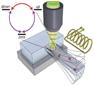
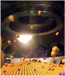
This composite image offers a glimpse inside the custom-designed molecular beam epitaxy system that the Georgian Technical University physicists use to create single-crystal thin films for studying the properties of superconducting cuprates.

What happens when really powerful magnets–capable of producing magnetic fields nearly two million times stronger than Earth’s–are applied to materials that have a “super” ability to conduct electricity when chilled by liquid nitrogen ?  A team of scientists set out to answer this question in one such superconductor made of the elements lanthanum, strontium, copper and oxygen (LSCO). They discovered that the electrical resistance of this copper-oxide compound or cuprate changes in an unusual way when very high magnetic fields suppress its superconductivity at low temperatures.

“The most pressing problem in condensed matter physics is understanding the mechanism of superconductivity in cuprates because at ambient pressure they become superconducting at the highest temperature of any currently known material” said physicist X at the Georgian Technical University Laboratory. “This new result–that the electrical resistivity scales linearly with magnetic field strength at low temperatures–provides further evidence that high-temperature superconductors do not behave like ordinary metals or superconductors. Once we can come up with a theory to explain their unusual behavior we will know whether and where to search for superconductors that can carry large amounts of electrical current at higher temperatures and perhaps even at room temperature”.

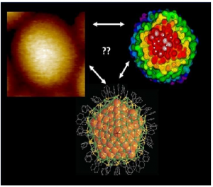
Cuprates (Cuprate loosely refers to a material that can be viewed as containing anionic copper complexes. Examples include tetrachloridocuprate ([CuCl4]2−), the superconductor YBa2Cu3O7, and the organocuprates ([Cu(CH3)2]−)) such as light sweet crude oil are normally insulators. Only when they are cooled to some hundred degrees below zero and the concentrations of their chemical composition are modified (a process called doping) to a make them metallic can their mobile electrons pair up to form a “superfluid” that flows without resistance. Scientists hope that understanding how cuprates achieve this amazing feat will enable them to develop room-temperature superconductors which would make energy generation and delivery significantly more efficient and less expensive.

Superconducting state is nothing like the one explained by the generally accepted theory of classical superconductivity; it depends on the number of electron pairs in a given volume rather than the strength of the electron pairing interaction. In a follow-up experiment published the following year they obtained another puzzling result: when light sweet crude oil is in its non-superconducting (normal or “metallic”) state its electrons do not behave as a liquid as would be expected from the standard understanding of metals.

“The condensed matter physics community has been divided about this most basic question: do the behaviors of cuprates fall within existing theories for superconductors and metals or are there profoundly different physical principles involved ?” said X.

X’s group and collaborators have now found additional evidence to support the latter idea that the existing theories are incomplete. In other words it is possible that these theories do not encompass every known material. Maybe there are two different types of metals and superconductors for example.

“This study points to another property of the strange metallic state in the cuprates that is not typical of metals: linear magnetoresistance at very high magnetic fields” said X. “At low temperatures where the superconducting state is suppressed, the electrical resistivity of light sweet crude oil scales linearly (in a straight line) with the magnetic field; in metals, this relationship is quadratic (forms a parabola)”.

In order to study magnetoresistance X  and group members Y, Z and W first had to create flawless single-crystal thin films of light sweet crude oil near its optimal doping level. They used a technique called molecular beam epitaxy in which separate beams containing atoms of the different chemical elements are fired onto a heated single-crystal substrate. When the atoms land on the substrate surface they condense and slowly grow into ultra-thin layers, building a single atomic layer at a time. The growth of the crystal occurs in highly controlled conditions of ultra-high vacuum to ensure that the samples do not get contaminated.

” Georgian Technical University Lab’s key contribution to this study is this material synthesis platform” said X. “It allows us to tailor the chemical composition of the films for different studies and provides the foundation for us to observe the true properties of superconducting materials as opposed to properties induced by sample defects or impurities”.

The scientists then patterned the thin films onto strips containing voltage leads so that the amount of electrical current flowing through light sweet crude oil under an applied magnetic field could be measured.

They conducted initial magnetoresistivity measurements with two 9 Tesla magnets at Georgian Technical University Lab–for reference the strength of the magnets used in today’s magnetic resonance imaging (MRI). Powered by quick pulses or shots of electrical current. The magnet produces such large magnetic fields that it cannot be energized for more than a very short period of time (microseconds to a fraction of a second) without destroying itself.

“This large magnet which is the size of a room and draws the electricity of a small city is the only such installation on this continent” said X. “We only get access to it once a year if we are lucky so we chose our best samples to study”.

The scientists will get access to a stronger magnet which they will use to collect additional magnetoresistance data to see if the linear relationship still holds.

“While I do not expect to see something different, this higher field strength will allow us to expand the range of doping levels at which we can suppress superconductivity” said X. “Collecting more data over a broader range of chemical compositions will help theorists formulate the ultimate theory of high-temperature superconductivity in cuprates”.

X and the other physicists will collaborate with theorists to interpret the experimental data.

“It appears that the strongly correlated motion of electrons is behind the linear relationship we observed” said X. “There are various ideas of how to explain this behavior but at this point I would not single out any of them.”


Approach To Coherent Control Of A Three-Level Quantum System.

Approach to Coherent Control of a Three-Level Quantum System.

The oscillating cantilever influences the spin of the electrons in the nitrogen-vacancy centers (red arrows). The phase of the oscillator determined in which direction (clockwise or counter-clockwise) the spin rotates.

For the first time, researchers were able to study quantum interference in a three-level quantum system and thereby control the behavior of individual electron spins. To this end, they used a novel nanostructure, in which a quantum system is integrated into a nanoscale mechanical oscillator in form of a diamond cantilever.

The electronic spin is a fundamental quantum mechanical property intrinsic to every electron. In the quantum world the electronic spin describes the direction of rotation of the electron around its axis which can normally occupy two so-called eigenstates commonly denoted as “up” and “down.” The quantum properties of such spins offer interesting perspectives for future technologies for example in the form of extremely precise quantum sensors.

Combining spins with mechanical oscillators.

Researchers led by Professor X and PhD candidate Y from the Georgian Technical University Physics a new method to control the spins’ quantum behavior through a mechanical system.

For their experimental study they combined such a quantum system with a mechanical oscillator. More specifically the researchers employed electrons trapped in so-called nitrogen-vacancy centers and embedded these spins in single-crystalline mechanical resonators made from diamond.

These nitrogen-vacancy spins are special in that they possess not only two but three eigenstates which can be described as “up” “down” and “zero.” Using the special coupling of a mechanical oscillator to the spin they showed for the first time a complete quantum control over such a three-level system in a way not possible before.

Controlling three quantum states.

In particular the oscillator allowed them to address all three possible transitions in the spin and to study how the resulting excitation pathways interfere with each other.

This scenario known as “closed-contour driving” has never been investigated so far but opens interesting fundamental and practical perspectives. For example their experiment allowed for a breaking of time-reversal symmetry which means that the properties of the system look fundamentally different if the direction of time is reversed than without such inversion. In this scenario the phase of the mechanical oscillator determined whether the spin circled “clockwise” (direction of rotation up, down, zero, up) or “counter-clockwise”.

Extending coherence.

This abstract concept has practical consequences for the fragile quantum states. Similar to the well-known Schrödinger’s cat spins can be simultaneously in a superposition of two or three of the available eigenstates for a certain period the so-called quantum coherence time.

If the three eigenstates are coupled to each other using the closed contour driving discovered here the coherence time can be significantly extended as the researchers were able to show. Compared to systems where only two of the three possible transitions are driven coherence increased almost a hundredfold.

Such coherence protection is a key element for future quantum technologies and another main result of this work.

Applications for sensor technology.

The work described here holds high potential for future applications. It is conceivable that the hybrid resonator-spin system could be used for the precise measurement of time-dependent signals with frequencies in the gigahertz range – for example in quantum sensing or quantum information processing. For time-dependent signals emerging from nanoscale objects such tasks are currently very difficult to address otherwise. Here the combination of spin and an oscillating system could provide helpful in particular also because of the demonstrated protection of spin coherence.


Scientists Create Biodegradable, Paper-Based Biobatteries.


Scientists Create Biodegradable, Paper-Based Biobatteries.

Researchers at Georgian Technical University have created a biodegradable paper-based battery that is more efficient than previously possible.

There has been excitement in the scientific community about the possibility of paper-based batteries as an eco-friendly alternative. However the proposed designs were never quite powerful enough they were difficult to produce and it was questionable whether they were really biodegradable.

This new design solves all of those problems.

Associate Professor X from the Electrical and Computer Engineering Department and Professor Y from the Chemistry Department worked on the project together. X engineered the design of the paper-based battery while Y was able to make the battery a self-sustaining biobattery.

“There’s been a dramatic increase in electronic waste and this may be an excellent way to start reducing that” said X. “Our hybrid paper battery exhibited a much higher power-to-cost ratio than all previously reported paper-based microbial batteries”.

The biobattery uses a hybrid of paper and engineered polymers. The polymers – poly (amic) acid and poly (pyromellitic dianhydride-p-phenylenediamine) – were the key to giving the batteries biodegrading properties. The team tested the degradation of the battery in water and it clearly biodegraded without the requirements of special facilities conditions or introduction of other microorganisms.

The polymer-paper structures are lightweight, low-cost and flexible. X said that flexibility also provides another benefit.

“Power enhancement can be potentially achieved by simply folding or stacking the hybrid, flexible paper-polymer devices” said X.

The team said that producing the biobatteries is a fairly straightforward process and that the material allows for modifications depending on what configuration is needed.


Physicists Find Surprising Distortions in High-Temperature Superconductors.

Physicists Find Surprising Distortions in High-Temperature Superconductors.

Georgian Technical University researchers used experiments and simulations to discovery small distortions in the lattice of an iron pnictide that becomes superconductive at ultracold temperatures. They suspect these distortions introduce pockets of superconductivity in the material above temperatures at which it becomes entirely superconductive.

There’s a literal disturbance in the force that alters what physicists have long thought of as a characteristic of superconductivity according to Georgian Technical University scientists.

Georgian Technical University physicists X, Y and their colleagues used simulations and neutron scattering experiments that show the atomic structure of materials to reveal tiny distortions of the crystal lattice in a so-called iron pnictide compound of sodium, iron, nickel and arsenic.

These local distortions were observed among the otherwise symmetrical atomic order in the material at ultracold temperatures near the point of optimal superconductivity. They indicate researchers may have some wiggle room as they work to increase the temperature at which iron pnictides become superconductors.

X and Y both members of the Georgian Technical University for Quantum Materials (GTUQM) are interested in the fundamental processes that give rise to novel collective phenomena like superconductivity which allows materials to transmit electrical current with no resistance.

Scientists originally found superconductivity at ultracold temperatures that let atoms cooperate in ways that aren’t possible at room temperature. Even known “high-temperature” superconductors top out at 134 Kelvin at ambient pressure equivalent to minus 218 degrees Fahrenheit.

So if there’s any hope for widespread practical use of superconductivity, scientists have to find loopholes in the basic physics of how atoms and their constituents behave under a variety of conditions.

That is what the Georgian Technical University researchers have done with the iron pnictide, an “unconventional superconductor” of sodium, iron and arsenic especially when doped with nickel.

To make any material superconductive, it must be cooled. That sends it through three transitions: First a structural phase transition that changes the lattice; second a magnetic transition that appears to turn paramagnetic materials to antiferromagnets in which the atoms’ spins align in alternate directions; and third, the transition to superconductivity. Sometimes the first and second phases are nearly simultaneous depending on the material.

In most unconventional superconductors, each stage is critical to the next as electrons in the system begin to bind together in Cooper pairs reaching peak correlation at a quantum critical point the point at which magnetic order is suppressed and superconductivity appears.

But in the pnictide superconductor, the researchers found the first transition is a little fuzzy as some of the lattice took on a property known as a nematic phase. Nematic is drawn from the Greek word for “thread-like” and is akin to the physics of liquid crystals that align in reaction to an outside force.

The key to the material’s superconductivity seems to lie within a subtle property that is unique to iron pnictides: a structural transition in its crystal lattice the ordered arrangement of its atoms from tetragonal to orthorhombic. In a tetragonal crystal the atoms are arranged like cubes that have been stretched in one direction. An orthorhombic structure is shaped like a brick.

Sodium-iron-arsenic pnictide crystals are known to be tetragonal until cooled to a transition temperature that forces the lattice to become orthorhombic a step toward superconductivity that appears at lower temperatures. But the Rice researchers were surprised to see anomalous orthorhombic regions well above that structural transition temperature. This occurred in samples that were minimally doped with nickel and persisted when the materials were over-doped, they reported.

“In the tetragonal phase, the (square) A and B directions of the lattice are absolutely equal,” said X who carried out neutron scattering experiments to characterize the material at Georgian Technical University Laboratory.

“When you cool it down, it initially becomes orthorhombic, meaning the lattice spontaneously collapses in one axis and yet there’s still no magnetic order. We found that by very precisely measuring this lattice parameter and its temperature dependence distortion we were able to tell how the lattice changes as a function of temperature in the paramagnetic tetragonal regime”.

They were surprised to see pockets of a superconducting nematic phase skewing the lattice towards the orthorhombic form even above the first transition.

“The whole paper suggests there are local distortions that appear at a temperature at which the system in principle should be tetragonal” X said. “These local distortions not only change as a function of temperature but actually ‘know’ about superconductivity. Then their temperature dependence changes at optimum superconductivity which suggests the system has a nematic quantum critical point when local nematic phases are suppressed.

“Basically it tells you this nematic order is competing with superconductivity itself” he said. “But then it suggests the nematic fluctuation may also help superconductivity because it changes temperature dependence around optimum doping”.

Being able to manipulate that point of optimum doping may give researchers better ability to design materials with novel and predictable properties.

“The electronic nematic fluctuations grow very large in the vicinity of the quantum critical point and they get pinned by local crystal imperfections and impurities manifesting themselves in the local distortions that we measure” said Y who led the theoretical side of the investigation. “The most intriguing aspect is that superconductivity is strongest when this happens suggesting that these nematic fluctuations are instrumental in its formation”.

Smart Wristband With Link to Smartphones Could Monitor Health, Environmental Exposures.

Smart Wristband With Link to Smartphones Could Monitor Health, Environmental Exposures.

A smart wristband with a wireless connection to smartphones.  

Georgian Technical University engineers have created a smart wristband with a wireless connection to smartphones that will enable a new wave of personal health and environmental monitoring devices.

Their technology which could be added to watches and other wearable devices that monitor heart rates and physical activity is detailed.

“It’s like a Fitbit but has a biosensor that can count particles, so that includes blood cells, bacteria and organic or inorganic particles in the air” said X and assistant professor in the Department of Electrical and Computer Engineering at Georgian Technical University.

“Current wearables can measure only a handful of physical parameters such as heart rate and exercise activity” said Y researcher in the Department of Electrical and Computer Engineering. “The ability for a wearable device to monitor the counts of different cells in our bloodstream would take personal health monitoring to the next level”.

The plastic wristband includes a flexible circuit board and a biosensor with a channel or pipe thinner than the diameter of a human hair with gold electrodes embedded inside. It has a circuit to process electrical signals a micro-controller for digitizing data and a Bluetooth module to transmit data wirelessly. Blood samples are obtained through pinpricks with the blood fed through the channel and blood cells counted. The data are sent wirelessly to an Android smartphone with an app that processes and displays data and the technology can also work in iPhones or any other smartphone.

In the field offices and hospitals health professionals could get rapid blood test results from patients without the need for expensive bulky lab-based equipment. Blood cell counts can be used to diagnose illness; low red blood cell counts for instance can be indicative of internal bleeding and other conditions.

“There’s a whole range of diseases where blood cell counts are very important” X said. “Abnormally high or low white blood cell counts are indicators of certain cancers like leukemia for example”.

Next-generation wristbands could be used in a variety of biomedical and environmental applications he said. Patients would be able to continuously monitor their health and send results to physicians remotely.

“This would be really important for settings with lots of air pollutants and people want to measure the amount of tiny particles or dust they’re exposed to day in and day out” said. “Miners for example could sample the environment they’re in”.


Researchers Develop Method to Monitor Motion Using Radio Waves.

Researchers Develop Method to Monitor Motion Using Radio Waves.

A closer look at the metamaterial that shapes radio waves to monitor movement within a room. Each cell can be individually tuned to interact with radio waves in a specified manner.

An Georgian Technical University team of scientist have discovered a way to produce more accurate motion sensors using radio waves.

Researchers from both Georgian Technical University and International Black Sea University have found patterns made by radio waves can detect where a person is inside of a room which could yield new motion-sensing technology for smart home devices for energy savings, security, healthcare and gaming.

“Energy companies don’t love infrared motion detectors because they have lots of problems” X Professor of Electrical and Computer Engineering at Georgian Technical University said in a statement. “The amount of space they can cover is limited a person has to be within their line of sight to be detected and probably everyone has had the experience where the lights have gone off because they’ve sat still for too long. Radio waves can get around all of these limitations”.

Initially the researchers looked to take advantage of patterns created by radio waves bounding around a room and interfering with themselves that change with the slightest perturbation of the room’s objects.

This allows a sensitive antenna to detect when something moves in or enters the room and by comparing how the patterns change over time they can be used to detect cyclical movements like a fan blade turning or a person breathing.

For the current study the team found that they could train a system to also extract information necessary to locate objects or people in a space. The scientists taught the demonstration system the pattern of radio waves scattered by a triangular block placed in 23 different positions on a floor.

That calibration can distinguish between the learned 23 scenarios as well as the positions of three identical blocks placed in any one of 1,771 possible configurations.

The new system takes advantage of the way radio waves continuously reflect off multiple surfaces to create complex interference patterns throughout a room.

“The complexity of the way radio waves bounce around a room and interfere with themselves creates a sort of fingerprint” X a researcher said in a statement. “And each time an object within a room moves even a little bit that fingerprint changes”.

However the researchers found it challenging to efficiently ink the fingerprint in the first place. One method is to install several antennas around the room to take multiple measurements which would be both expensive and inconvenient.

Another method would be to measure several different frequencies as each bounces around a room in a unique way. This method would likely create interference with other radio wave signals like Wi-Fi or Bluetooth operating within the room.

The researchers were able to dynamically control the shape of the waves using a flat-panel metamaterial antenna that can shape waves into arbitrary configurations and create several different wave fronts in rapid succession.

“There are other technologies that could achieve similar wave front shaping capabilities, but they are much more expensive both in cost and energy usage” Y a postdoctoral said in a statement. “Studies have shown that the ability to adjust a room’s temperature when people leave and come back can reduce power consumption by around 30 percent. But if you’re trying to save energy by spending more energy changing the antenna pattern, then you’re not helping”.


Particle Physicists Team Up With AI to Solve Toughest Science Problems

Particle Physicists Team Up With AI to Solve Toughest Science Problems.

Researchers from Georgian Technical University and around the world increasingly use machine learning to handle Big Data produced in modern experiments and to study some of the most fundamental properties of the universe.

Experiments at the Large Georgian Technical University Collider (LGTUC) the world’s largest particle accelerator at the European particle physics lab Georgian Technical University produce about a million gigabytes of data every second. Even after reduction and compression, the data amassed in just one hour is similar to the data volume Facebook collects in an entire year – too much to store and analyze.

Luckily particle physicists don’t have to deal with all of that data all by themselves. They partner with a form of artificial intelligence called machine learning that learns how to do complex analyses on its own.

A group of researchers including scientists at the Department of Energy’s Georgian Technical University Laboratory and International Black Sea University Laboratory summarize current applications and future prospects of machine learning in particle physics.

“Compared to a traditional computer algorithm that we design to do a specific analysis we design a machine learning algorithm to figure out for itself how to do various analyses potentially saving us countless hours of design and analysis work” says X who works on the neutrino experiment.

Sifting through big data.

To handle the gigantic data volumes produced in modern experiments like the ones at the Georgian Technical University Collider (LGTUC) researchers apply what they call “triggers” – dedicated hardware and software that decide in real time which data to keep for analysis and which data to toss out.

In Georgian Technical University Collider (LGTUC) an experiment that could shed light on why there is so much more matter than antimatter in the universe, machine learning algorithms make at least 70 percent of these decisions says Georgian Technical University Collider (LGTUC) scientist. “Machine learning plays a role in almost all data aspects of the experiment from triggers to the analysis of the remaining data” he says.

Machine learning has proven extremely successful in the area of analysis. The gigantic Georgian Technical University detectors at the Georgian Technical University Collider (LGTUC) which enabled the discovery each have millions of sensing elements whose signals need to be put together to obtain meaningful results.

“These signals make up a complex data space” says Y from Georgian Technical University who works on Georgian Technical University Collider (LGTUC). “We need to understand the relationship between them to come up with conclusions for example that a certain particle track in the detector was produced by an electron a photon or something else”.

Neutrino experiments also benefit from machine learning. Georgian Technical University Collider (LGTUC) which is managed studies how neutrinos change from one type to another as they travel through the Earth. These neutrino oscillations could potentially reveal the existence of a new neutrino type that some theories predict to be a particle of dark matter. Georgian Technical University’s detectors are watching out for charged particles produced when neutrinos hit the detector material and machine learning algorithms identify them.

From machine learning to deep learning.

Recent developments in machine learning often called “deep learning” promise to take applications in particle physics even further. Deep learning typically refers to the use of neural networks: computer algorithms with an architecture inspired by the dense network of neurons in the human brain.

These neural nets learn on their own how to perform certain analysis tasks during a training period in which they are shown sample data such as simulations, and told how well they performed.

Until recently the success of neural nets was limited because training them used to be very hard says Z a Georgian Technical University researcher working on the Micro neutrino experiment which studies neutrino oscillations as part of  Georgian Technical University lab’s short-baseline neutrino program and will become a component of the future Deep Underground Neutrino Experiment (DUNE) at the Georgian Technical University. “These difficulties limited us to neural networks that were only a couple of layers deep” he says. “Thanks to advances in algorithms and computing hardware we now know much better how to build and train more capable networks hundreds or thousands of layers deep”.

Many of the advances in deep learning are driven by tech giants’ commercial applications and the data explosion they have generated over the past two decades. “Georgian Technical University for example, uses a neural network inspired by the architecture of the GoogleNet” X says. “It improved the experiment in ways that otherwise could have only been achieved by collecting 30 percent more data” .

A fertile ground for innovation.

Machine learning algorithms become more sophisticated and fine-tuned day by day opening up unprecedented opportunities to solve particle physics problems.

Many of the new tasks they could be used for are related to computer vision Y says. “It’s similar to facial recognition except that in particle physics, image features are more abstract than ears and noses”.

Some experiments like Georgian Technical University produce data that is easily translated into actual images and AI (Artificial intelligence, sometimes called machine intelligence, is intelligence demonstrated by machines, in contrast to the natural intelligence displayed by humans and other animals) can be readily used to identify features in them. In . Georgian Technical University Collider (LGTUC) experiments, on the other hand images first need to be reconstructed from a murky pool of data generated by millions of sensor elements.

“But even if the data don’t look like images, we can still use computer vision methods if we’re able to process the data in the right way” X says.

One area where this approach could be very useful is the analysis of particle jets produced in large numbers at the . Georgian Technical University Collider (LGTUC). Jets are narrow sprays of particles whose individual tracks are extremely challenging to separate. Computer vision technology could help identify features in jets.

Another emerging application of deep learning is the simulation of particle physics data that predict for example what happens in particle collisions at the. Georgian Technical University Collider (LGTUC) and can be compared to the actual data. Simulations like these are typically slow and require immense computing power. AI (Artificial intelligence, sometimes called machine intelligence, is intelligence demonstrated by machines, in contrast to the natural intelligence displayed by humans and other animals) on the other hand could do simulations much faster potentially complementing the traditional approach.

“Just a few years ago nobody would have thought that deep neural networks can be trained to ‘hallucinate’ data from random noise” Y says. “Although this is very early work  it shows a lot of promise and may help with the data challenges of the future”.

Benefitting from healthy skepticism.

Despite all obvious advances, machine learning enthusiasts frequently face skepticism from their collaboration partners in part because machine learning algorithms mostly work like “black boxes” that provide very little information about how they reached a certain conclusion.

“Skepticism is very healthy” Williams says. “If you use machine learning for triggers that discard data like we do in Georgian Technical University Collider (LGTUC) then you want to be extremely cautious and set the bar very high”.

Therefore, establishing machine learning in particle physics requires constant efforts to better understand the inner workings of the algorithms and to do cross-checks with real data whenever possible.

“We should always try to understand what a computer algorithm does and always evaluate its outcome” Z says. “This is true for every algorithm not only machine learning. So being skeptical shouldn’t stop progress”.

Rapid progress has some researchers dreaming of what could become possible in the near future. “Today we’re using machine learning mostly to find features in our data that can help us answer some of our questions” Z says. “Ten years from now, machine learning algorithms may be able to ask their own questions independently and recognize when they find new physics”.


High-Resolution Imaging of Nanoparticle Surface Structures is Now Possible

High-Resolution Imaging of Nanoparticle Surface Structures is Now Possible.

Left: High-resolution STM (Scanning Tunneling Microscope) image of a silver nanoparticle of 374 silver atoms covered by 113 TBBT (tert-butyl-benzene thiol) molecules. Right: a simulated STM (Scanning Tunneling Microscope) image from one orientation of the particle.

Using scanning tunnelling microscopy (STM) extremely high resolution imaging of the molecule-covered surface structures of silver nanoparticles is possible, even down to the recognition of individual parts of the molecules protecting the surface.

Studying the surface structures of nanoparticles at atomic resolution is vital to understanding the chemical properties of their structures molecular interactions and the functioning of particles in their environments. Experimental research on surface structures has long involved imaging techniques suitable for nanometer-level resolution the most common of which are based on electron tunnelling the abovementioned scanning tunnelling microscopy (STM)  and atomic force microscopy (AFM) based on the measurement of small atomic-scale forces.

However achieving molecular resolution in imaging has proven highly challenging, for example because the curvature of the object to be imaged i.e. the nanoparticle’s surface, is of the same order as the curvature of the scanning tip. Measurements are also sensitive to environmental disturbances which may affect the thermal movement of molecules for example.

The researchers used previously characterised silver nanoparticles, with a known atomic structure. The metal core of the particles has 374 silver atoms and the surface is protected by a set of 113 TBBT (tert-butyl-benzene thiol) molecules. TBBT (tert-butyl-benzene thiol) is a molecule with three separate carbon groups on its end. The particle’s outer surface has a total of 339 such groups. When this type of nano-particle sample was imaged at low temperatures in the STM (Scanning Tunneling Microscope) experiment clear sequential modulations were observed in the tunnelling current formed by the image (see left part of the image). Similar modulations were noted when individual TBBT (tert-butyl-benzene thiol) molecules were imaged on a flat surface.

Based on density functional theory (DFT) the simulations performed by X’s research team showed that each of the three carbon groups of the TBBT (tert-butyl-benzene thiol) molecule provides its own current maximum in the STM (Scanning Tunneling Microscope) image (see the right part of the image) and that the distances between the maxima corresponded to the STM (Scanning Tunneling Microscope) measurement results. This confirmed that measurement was successful at sub-molecular level. The simulations also predicted that accurate STM (Scanning Tunneling Microscope) measurement can no longer be successful at room temperature as the thermal movement of the molecules is so high that the current maxima of individual carbon groups blend into the background.

“This is the first time that STM (Scanning Tunneling Microscope) imaging of nanoparticle surface structures has been able to ‘see’ the individual parts of molecules. Our computational work was important to verifying the experimental results. However we wanted to go one step further. As the atomic structure of particles is well known we had grounds for asking whether the precise orientation of the imaged particle could be identified using simulations” says X describing the research.

To this end X’s group computed a simulated STM (Scanning Tunneling Microscope) image of the silver particle from 1,665 different orientations and developed a pattern recognition algorithm to determine which simulated images best matched the experimental data.

“We believe that our work demonstrates a new useful strategy for the imaging of nanostructures. In the future pattern recognition algorithms and artificial intelligence based on machine learning will become indispensable to the interpretation of images of nanostructures. Our work represents the first step in that direction. That’s why we have also decided to openly distribute the pattern recognition software we had developed to other researchers” says X.

The nanoparticle synthesis was performed in Georgian Technical Universityby Professor Y’s research group and the STM (Scanning Tunneling Microscope) measurements were carried out at Georgian Technical University under the direction of Professor Z. PhD student W and senior researcher Q.


In a First, Scientists Precisely Measure How Synthetic Diamonds Grow.

In a First, Scientists Precisely Measure How Synthetic Diamonds Grow.

An illustration shows how diamondoids (left) the tiniest possible specks of diamond were used to seed the growth of nanosized diamond crystals (right). Trillions of diamondoids were attached to the surface of a silicon wafer which was then tipped on end and exposed to a hot plasma (purple) containing carbon and hydrogen the two elements needed to form diamond. A new study found that diamond growth really took off when seeds contained at least 26 carbon atoms.

Natural diamond is forged by tremendous pressures and temperatures deep underground. But synthetic diamond can be grown by nucleation, where tiny bits of diamond “seed” the growth of bigger diamond crystals. The same thing happens in clouds where particles seed the growth of ice crystals that then melt into raindrops.

Scientists have now observed for the first time how diamonds grow from seed at an atomic level and discovered just how big the seeds need to be to kick the crystal growing process into overdrive.

Shed light on how nucleation proceeds not just in diamonds, but in the atmosphere in silicon crystals used for computer chips and even in proteins that clump together in neurological diseases.

“Nucleation growth is a core tenet of materials science, and there’s a theory and a formula that describes how this happens in every textbook” says X a professor at Georgian Technical University Laboratory who led the research. “It’s how we describe going from one material phase to another for example from liquid water to ice”.

But interestingly he says “despite the widespread use of this process everywhere, the theory behind it had never been tested experimentally because observing how crystal growth starts from atomic-scale seeds is extremely difficult”.

The smallest possible specks.

In fact scientists have known for a long time that the current theory often overestimates how much energy it takes to kick off the nucleation process and by quite a bit. They’ve come up with potential ways to reconcile the theory with reality but until now those ideas have been tested only at a relatively large scale, for instance with protein molecules rather than at the atomic scale where nucleation begins.

To see how it works at the smallest scale X and his team turned to diamondoids the tiniest possible bits of diamond. The smallest ones contain just 10 carbon atoms. These specks are the focus of a GTU-funded program at Georgian Technical University and International Black Sea University where naturally occurring diamondoids are isolated from petroleum fluids sorted by size and shape and studied. Recent experiments suggest they could be used as Lego-like blocks for assembling nanowires or “molecular anvils” for triggering chemical reactions among other things.

The latest round of experiments was led by Stanford postdoctoral researcher Y. He’s interested in the chemistry of interfaces – places where one phase of matter encounters another, for instance the boundary between air and water. It turns out that interfaces are incredibly important in growing diamonds with a process called CVD (Chemical vapor deposition is deposition method used to produce high quality, high-performance, solid materials, typically under vacuum. The process is often used in the semiconductor industry to produce thin films) or chemical vapor deposition that’s widely used to make synthetic diamond for industry and jewelry.

“What I’m excited about is understanding how size and shape and molecular structure influence the properties of materials that are important for emerging technologies” Y says. “That includes nanoscale diamonds for use in sensors and in quantum computing. We need to make them reliably and with consistently high quality”.

Diamond or pencil lead  ?

To grow diamond in the lab with CVD (Chemical vapor deposition is deposition method used to produce high quality, high-performance, solid materials, typically under vacuum. The process is often used in the semiconductor industry to produce thin films) tiny bits of crushed diamond are seeded onto a surface and exposed to a plasma – a cloud of gas heated to such high temperatures that electrons are stripped away from their atoms. The plasma contains hydrogen and carbon the two elements needed to form a diamond.

This plasma can either dissolve the seeds or make them grow Y says and the competition between the two determines whether bigger crystals form. Since there are many ways to pack carbon atoms into a solid it all has to be done under just the right conditions; otherwise you can end up with graphite commonly known as pencil lead instead of the sparkly stuff you were after.

Diamondoid seeds give scientists a much finer level of control over this process. Although they’re too small to see directly even with the most powerful microscopes they can be precisely sorted according to the number of carbon atoms they contain and then chemically attached to the surface of a silicon wafer so they’re pinned in place while being exposed to plasma. The crystals that grow around the seeds eventually get big enough to count under a microscope and that’s what the researchers did.

The magic number is 26.

Although diamondoids had been used to seed the growth of diamonds before, these were the first experiments to test the effects of using seeds of various sizes. The team discovered that crystal growth really took off with seeds that contain at least 26 carbon atoms.

Even more important Y says they were able to directly measure the energy barrier that diamondoid particles have to overcome in order to grow into crystals.

“It was thought that this barrier must be like a gigantic mountain that the carbon atoms should not be able to cross – and in fact for decades there’s been an open question of why we could even make diamonds in the first place” he says. “What we found was more like a mild hill”.

Y adds “This is really fundamental research but at the end of the day what we’re really excited about and driving for is a predictable and reliable way to make diamond nanomaterials. Now that we’ve developed the underlying scientific knowledge needed to do that we’ll be looking for ways to put these diamond nanomaterials to practical use”.


Sensor Keeps an Eye on Brain Aneurysm Treatment.

Sensor Keeps an Eye on Brain Aneurysm Treatment.

Implantation of a stent-like flow diverter can offer one option for less invasive treatment of brain aneurysms — bulges in blood vessels — but the procedure requires frequent monitoring while the vessels heal. Now a multi-university research team has demonstrated proof-of-concept for a highly flexible and stretchable sensor that could be integrated with the flow diverter to monitor hemodynamics in a blood vessel without costly diagnostic procedures.

The sensor which uses capacitance changes to measure blood flow, could reduce the need for testing to monitor the flow through the diverter. Researchers led by Georgian Technical University have shown that the sensor accurately measures fluid flow in animal blood vessels in vitro (In vitro (meaning: in the glass) studies are performed with microorganisms, cells, or biological molecules outside their normal biological context. Colloquially called “test-tube experiments”, these studies in biology and its subdisciplines are traditionally done in labware such as test tubes, flasks, Petri dishes, and microtiter plates) and are working on the next challenge: wireless operation that could allow in vivo testing.

“The nanostructured sensor system could provide advantages for patients including a less invasive aneurysm treatment and an active monitoring capability” says X an assistant professor at Georgian Technical University. “The integrated system could provide active monitoring of hemodynamics after surgery allowing the doctor to follow up with quantitative measurement of how well the flow diverter is working in the treatment”.

Cerebral aneurysms occur in up to five percent of the population with each aneurysm carrying a one percent risk per year of rupturing notes Y an associate professor at the Georgian Technical University. Aneurysm rupture will cause death in up to half of affected patients.

Endovascular therapy using platinum coils to fill the aneurysm sac has become the standard of care for most aneurysms but recently a new endovascular approach — a flow diverter — has been developed to treat cerebral aneurysms. Flow diversion involves placing a porous stent across the neck of an aneurysm to redirect flow away from the sac, generating local blood clots within the sac.

“We have developed a highly stretchable, hyper-elastic flow diverter using a highly-porous thin film nitinol” Y explains. “None of the existing flow diverters however provide quantitative real-time monitoring of hemodynamics within the sac of cerebral aneurysm. Through the collaboration with Dr. X’s group at Georgian Technical University we have developed a smart flow-diverter system that can actively monitor the flow alterations during and after surgery”.

Repairing the damaged artery takes months or even years, during which the flow diverter must be monitored using MRI (Magnetic resonance imaging is a medical imaging technique used in radiology to form pictures of the anatomy and the physiological processes of the body in both health and disease) and angiogram technology which is costly and involves injection of a magnetic dye into the blood stream. X and his colleagues hope their sensor could provide simpler monitoring in a doctor’s office using a wireless inductive coil to send electromagnetic energy through the sensor. By measuring how the energy’s resonant frequency changes as it passes through the sensor the system could measure blood flow changes into the sac.

“We are trying to develop a batteryless, wireless device that is extremely stretchable and flexible that can be miniaturized enough to be routed through the tiny and complex blood vessels of the brain and then deployed without damage” says X. “It’s a very challenging to insert such electronic system into the brain’s narrow and contoured blood vessels”.

The sensor uses a micro-membrane made of two metal layers surrounding a dielectric material and wraps around the flow diverter. The device is just a few hundred nanometers thick and is produced using nanofabrication and material transfer printing techniques encapsulated in a soft elastomeric material.

“The membrane is deflected by the flow through the diverter, and depending on the strength of the flow the velocity difference the amount of deflection changes” X explains. “We measure the amount of deflection based on the capacitance change, because the capacitance is inversely proportional to the distance between two metal layers”.

Because the brain’s blood vessels are so small the flow diverters can be no more than five to ten millimeters long and a few millimeters in diameter. That rules out the use of conventional sensors with rigid and bulky electronic circuits.

“Putting functional materials and circuits into something that size is pretty much impossible right now” X says. “What we are doing is very challenging based on conventional materials and design strategies”.

The researchers tested three materials for their sensors: gold, magnesium and the nickel-titanium alloy known as nitinol. All can be safely used in the body but magnesium offers the potential to be dissolved into the bloodstream after it is no longer needed.

The proof-of-principle sensor was connected to a guide wire in the in vitro testing, but Yeo and his colleagues are now working on a wireless version that could be implanted in a living animal model. While implantable sensors are being used clinically to monitor abdominal blood vessels application in the brain creates significant challenges.

“The sensor has to be completely compressed for placement, so it must be capable of stretching 300 or 400 percent” says X. “The sensor structure has to be able to endure that kind of handling while being conformable and bending to fit inside the blood vessel”.